Pin configuration, Chip information – Rainbow Electronics MAX1845 User Manual
Page 23
MAX1845
Dual, High-Efficiency, Step-Down
Controller with Accurate Current Limit
______________________________________________________________________________________
23
through the inductor, through the input capacitor,
and back to the input.
• When trade-offs in trace lengths must be made, it’s
preferable to allow the inductor charging path to be
made longer than the discharge path. For example,
it’s better to allow some extra distance between the
input capacitors and the high-side MOSFET than to
allow distance between the inductor and the low-
side MOSFET or between the inductor and the out-
put filter capacitor.
• Route high-speed switching nodes (BST_, LX_, DH_,
and DL_) away from sensitive analog areas (REF,
ILIM_, FB_).
Layout Procedure
1) Place the power components first, with ground termi-
nals adjacent (sense resistor, C
IN
-, C
OUT
-, D1
anode). If possible, make all these connections on
the top layer with wide, copper-filled areas.
2) Mount the controller IC adjacent to the synchronous
rectifiers MOSFETs, preferably on the back side in
order to keep CS_, GND, and the DL_ gate-drive line
short and wide. The DL_ gate trace must be short
and wide, measuring 10 squares to 20 squares
(50mils to 100mils wide if the MOSFET is 1 inch from
the controller IC).
3) Group the gate-drive components (BST_ diode and
capacitor, V
DD
bypass capacitor) together near the
controller IC.
4) Make the DC-DC controller ground connections as
follows: Create a small analog ground plane (AGND)
near the IC. Connect this plane directly to GND
under the IC, and use this plane for the ground con-
nection for the REF and V
CC
bypass capacitors,
FB_, OVP, and ILIM_ dividers (if any). Do not con-
nect the AGND plane to any ground other than the
GND pin. Create another small ground island
(PGND), and use it for the V
DD
bypass capacitor,
placed very close to the IC. Connect the PGND
plane directly to GND from the outside of the IC.
5) On the board’s top side (power planes), make a star
ground to minimize crosstalk between the two sides.
The top-side star ground is a star connection of the
input capacitors, side 1 low-side MOSFET, and side
2 low-side MOSFET. Keep the resistance low
between the star ground and the source of the low-
side MOSFETs for accurate current limit. Connect
the top-side star ground (used for MOSFET, input,
and output capacitors) to the small PGND island with
a short, wide connection (preferably just a via).
Minimize crosstalk between side 1 and side 2 by
directing their switching ground currents into the star
ground with a notch as shown in Figure 10. If multi-
ple layers are available (highly recommended), cre-
ate PGND1 and PGND2 islands on the layer just
below the top-side layer (refer to the MAX1845 EV kit
for an example) to act as an EMI shield. Connect
each of these individually to the star-ground via,
which connects the top side to the PGND plane. Add
one more solid ground plane under the IC to act as
an additional shield, and also connect that to the
star-ground via.
6) Connect the output power planes directly to the out-
put filter capacitor positive and negative terminals
with multiple vias.
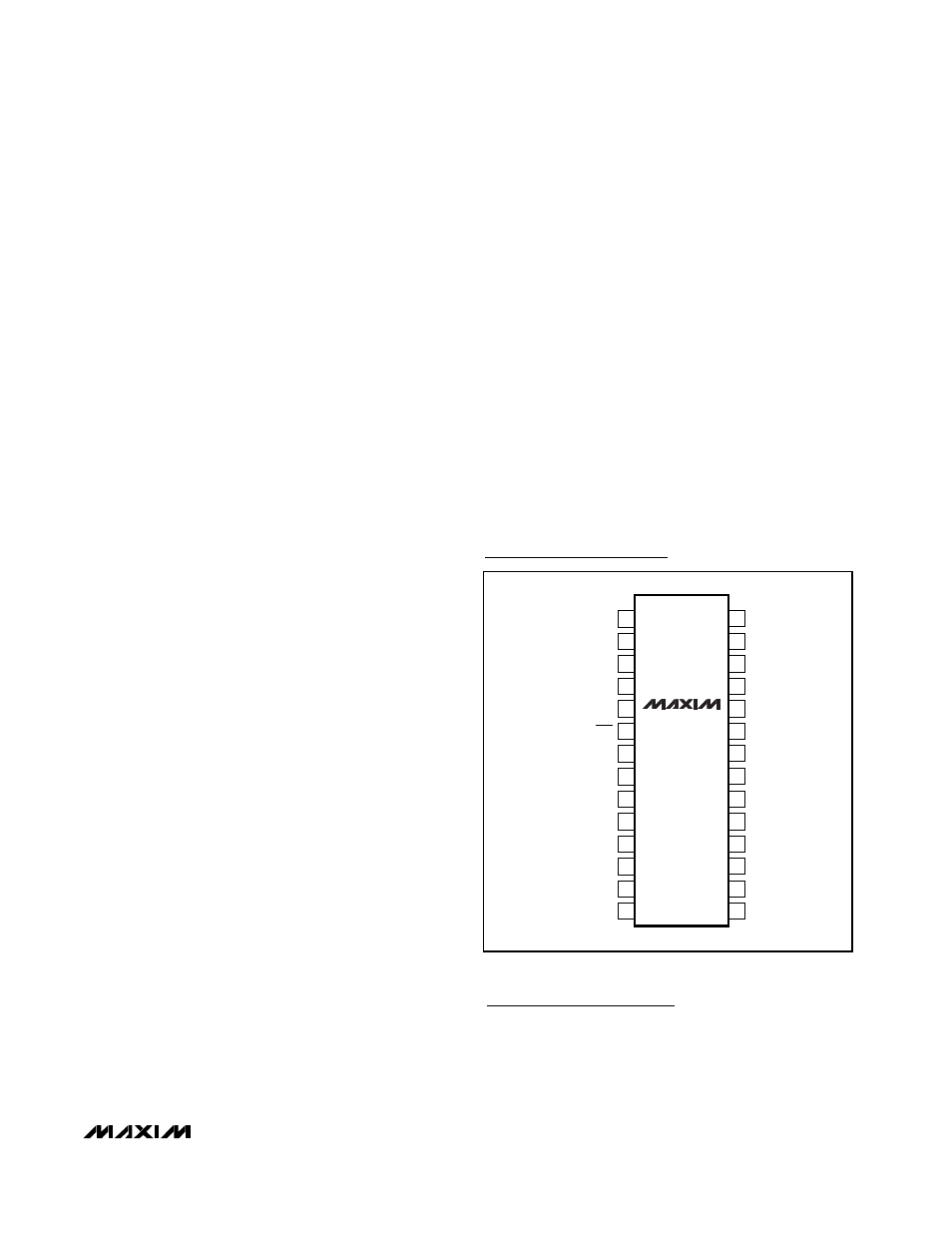
Pin Configuration
28
27
26
25
24
23
22
21
20
19
18
17
16
15
1
2
3
4
5
6
7
8
9
10
11
12
13
14
CS1
LX1
DH1
BST1
DL1
GND
OUT2
V
CC
V
DD
DL2
BST2
DH2
LX2
CS2
FB2
ILIM2
ON2
ON1
REF
UVP
OVP
PGOOD
SKIP
TON
V+
ILIM1
FB1
OUT1
QSOP
TOP VIEW
MAX1845
Chip Information
TRANSISTOR COUNT: 4795
PROCESS: BiCMOS