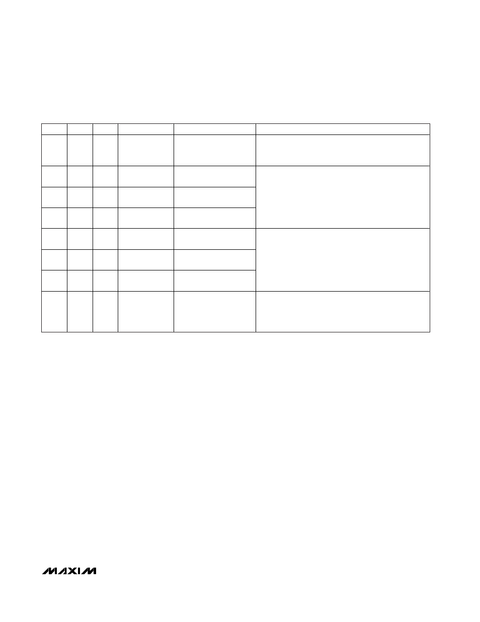
Table 3. operating mode truth table – Rainbow Electronics MAX1845 User Manual
Page 15

MAX1845
Dual, High-Efficiency, Step-Down
Controller with Accurate Current Limit
______________________________________________________________________________________
15
of multiple-output applications that use a flyback trans-
former or coupled inductor.
Current-Limit Circuit (ILIM_)
The current-limit circuit employs a unique “valley” current-
sensing algorithm. If the magnitude of the current-sense
signal at CS_ is above the current-limit threshold, the
PWM is not allowed to initiate a new cycle (Figure 5). The
actual peak current is greater than the current-limit
threshold by an amount equal to the inductor ripple cur-
rent. Therefore, the exact current-limit characteristic and
maximum load capability are a function of the sense
resistance, inductor value, and battery voltage.
There is also a negative current limit that prevents exces-
sive reverse inductor currents when V
OUT
is sinking cur-
rent. The negative current-limit threshold is set to
approximately 120% of the positive current limit and
therefore tracks the positive current limit when ILIM is
adjusted.
The current-limit threshold is adjusted with an internal
5µA current source and an external resistor at ILIM. The
current-limit threshold adjustment range is from 25mV
to 250mV. In the adjustable mode, the current-limit
threshold voltage is precisely 1/10 the voltage seen at
ILIM. The threshold defaults to 50mV when ILIM is con-
nected to V
CC
. The logic threshold for switchover to the
50mV default value is approximately V
CC
- 1V.
Carefully observe the PC board layout guidelines to
ensure that noise and DC errors do not corrupt the cur-
rent-sense signal seen by CS_ and GND. Mount or
place the IC close to the low-side MOSFET and sense
resistor with short, direct traces, making a Kelvin sense
connection to the sense resistor. In Figure 1, the
Schottky diodes (D1 and D2) provide current paths
parallel to the Q2/R
SENSE
and Q4/R
SENSE
current
paths, respectively. Accurate current sensing requires
D1/D2 to be off while Q2/Q4 conducts. Avoid large cur-
rent-sense voltages that, combined with the voltage
across Q2/Q4, would allow D1/D2 to conduct. If very
large sense voltages are used, connect D1/D2 in paral-
lel with Q2/Q4 only.
MOSFET Gate Drivers (DH_, DL_)
The DH and DL drivers are optimized for driving mod-
erate-size, high-side and larger, low-side power
MOSFETs. This is consistent with the low duty factor
seen in the notebook CPU environment, where a large
V
BATT
- V
OUT
differential exists. An adaptive dead-time
circuit monitors the DL output and prevents the high-
side FET from turning on until DL is fully off. There must
Table 3. Operating Mode Truth Table
ON1
ON2
SK IP
DL1/DL2
MODE
COMMENTS
GND
GND
X
High*/High*
Shutdown
Low-power shutdown state. If overvoltage protection is
enabled, DL1 and DL2 are forced to V
DD
, ensuring
overvoltage protection, I
CC
< 1µA (typ).
V
CC
GND
V
CC
Switching/High*
Run (PWM), Low Noise,
Side 1 Only
GND
V
CC
V
CC
High*/Switching
Run (PWM), Low Noise,
Side 2 Only
V
CC
V
CC
V
CC
Switching/
Switching
Run (PWM), Low Noise,
Both Sides Active
Low-noise, fixed frequency PWM at all load conditions.
Low noise, high I
Q
.
V
CC
GND
GND
Switching/High*
Run (PWM/PFM), Skip
Mode, Side 1 Only
GND
V
CC
GND
High*/Switching
Run (PWM/PFM), Skip
Mode, Side 2 Only
V
CC
V
CC
GND
Switching/
Switching
Run ( P W M /P FM ) , S ki p
M od e, Both S i d es Acti ve
Normal operation with automatic PWM/PFM switchover
for pulse skipping at light loads. Best light-load
efficiency.
V
CC
V
CC
X
High*/High*
Fault
Fault latch has been set by overvoltage protection circuit,
undervoltage protection circuit, or thermal shutdown.
Device will remain in fault mode until V
CC
power is
cycled or ON1/ON2 is toggled.
*DL_ high only if overvoltage protection enabled (see Output Overvoltage Protection section).
