Rainbow Electronics MAX1845 User Manual
Page 22

MAX1845
Dual, High-Efficiency, Step-Down
Controller with Accurate Current Limit
22
______________________________________________________________________________________
mount all of the power components on the top side of
the board, with connecting terminals flush against one
another.
Keep the high-current paths short, especially at the
ground terminals. This practice is essential for stable,
jitter-free operation. Short power traces and load con-
nections are essential for high efficiency. Using thick
copper PC boards (2oz vs. 1oz) can enhance full-load
efficiency by 1% or more. Correctly routing PC board
traces is a difficult task that must be approached in
terms of fractions of centimeters, where a single mil-
liohm of excess trace resistance causes a measurable
efficiency penalty.
Place the current-sense resistors close to the top-side
star-ground point (where the IC ground connects to the
top-side ground plane) to minimize current-sensing
errors. Avoid additional current-sensing errors by using
a Kelvin connection from CS_ pins to the sense resis-
tors.
The following guidelines are in order of importance:
• Keep the space between the ground connection of
the current-sense resistors short and near the via to
the IC ground pin.
• Minimize the resistance on the low-side path. The
low-side path starts at the ground of the low-side
FET, goes through the low-side FET, through the
inductor, through the output capacitor, and returns
to the ground of the low-side FET. Minimize the resis-
tance by keeping the components close together
and the traces short and wide.
• Minimize the resistance in the high-side path. This
path starts at V
IN
, goes through the high-side FET,
DL_
GND
OUT_
CS_
DH_
FB_
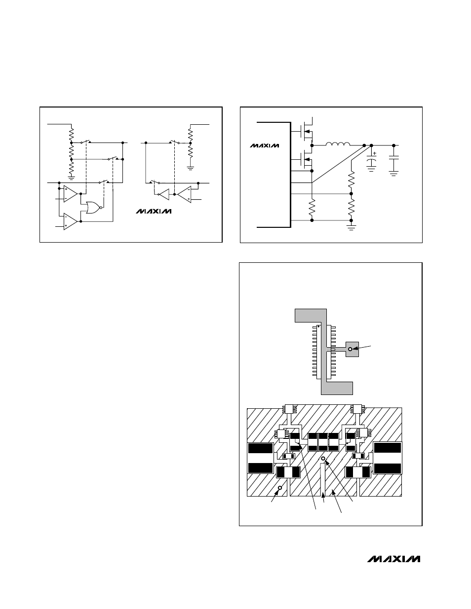
V
BATT
V
OUT
R1
R2
MAX1845
Figure 9. Setting V
OUT
with a Resistor-Divider
MAX1845
TO ERROR
AMP1
TO ERROR
AMP2
OUT2
FB2
0.1V
2V
0.1V
FB1
FIXED
2.5V
FIXED
1.5V
FIXED
1.8V
OUT1
Figure 8. Feedback Mux
AGND PLANE
AGND PLANE
PGND PLANE
VIA TO OUT1
VIA TO PGND PLANE AND IC GND
VIA TO CS1
NOTCH
V
IN
USE AGND PLANE TO:
- BYPASS V
CC
AND REF
- TERMINATE EXTERNAL FB, ILIM,
OVP DIVIDERS, IF USED
- PIN-STRAP CONTROL
INPUTS
USE PGND PLANE TO:
- BYPASS V
DD
- CONNECT IC GROUND
TO TOP-SIDE STAR GROUND
VIA TO TOP-SIDE
GROUND
TOP-SIDE GROUND PLANE
L2
L1
C1
C2
Q1
Q2
Q3
Q4
C
IN
C
IN
C
IN
D2
D1
Figure 10. PC Board Layout Example
