Rainbow Electronics MAX1845 User Manual
Page 20

MAX1845
Dual, High-Efficiency, Step-Down
Controller with Accurate Current Limit
20
______________________________________________________________________________________
Input Capacitor Selection
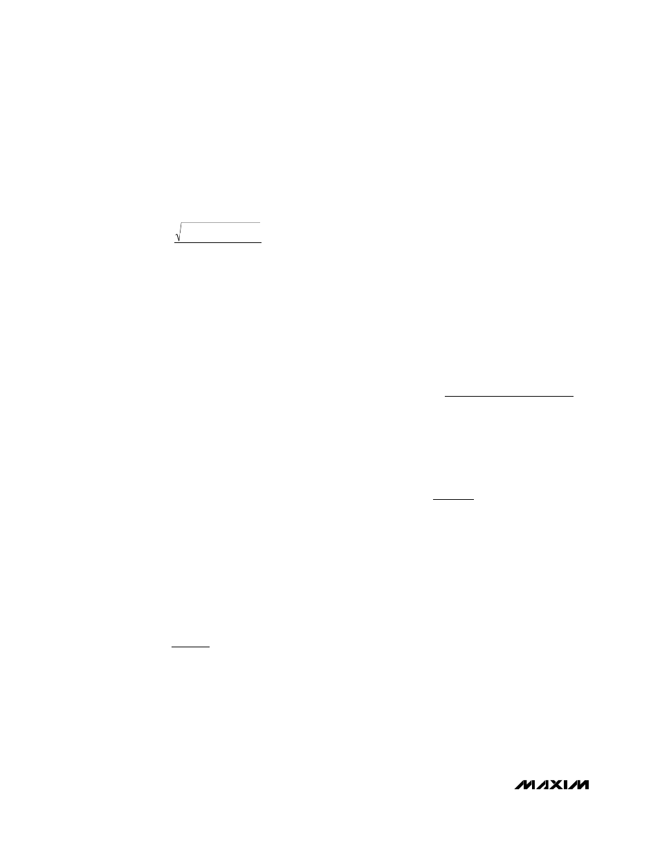
The input capacitor must meet the ripple current
requirement (I
RMS
) imposed by the switching currents.
Nontantalum chemistries (ceramic, aluminum, or OS-
CON) are preferred due to their resistance to power-up
surge currents:
Power MOSFET Selection
Most of the following MOSFET guidelines focus on the
challenge of obtaining high load-current capability
(>5A) when using high-voltage (>20V) AC adapters.
Low-current applications usually require less attention.
For maximum efficiency, choose a high-side MOSFET
(Q1) that has conduction losses equal to the switching
losses at the optimum battery voltage (15V). Check to
ensure that the conduction losses at the minimum
input voltage do not exceed the package thermal limits
or violate the overall thermal budget. Check to ensure
that conduction losses plus switching losses at the
maximum input voltage do not exceed the package
ratings or violate the overall thermal budget.
Choose a low-side MOSFET (Q2) that has the lowest
possible R
DS(ON)
, comes in a moderate to small pack-
age (i.e., SO-8), and is reasonably priced. Ensure that
the MAX1845 DL gate driver can drive Q2; in other
words, check that the gate is not pulled up by the high-
side switch turning on due to parasitic drain-to-gate
capacitance, causing cross-conduction problems.
Switching losses are not an issue for the low-side MOS-
FET since it is a zero-voltage switched device when
used in the buck topology.
MOSFET Power Dissipation
Worst-case conduction losses occur at the duty cycle
extremes. For the high-side MOSFET, the worst-case-
power dissipation (PD) due to resistance occurs at min-
imum battery voltage:
Generally, a small high-side MOSFET is desired in
order to reduce switching losses at high input voltages.
However, the R
DS(ON)
required to stay within package
power-dissipation limits often limits how small the MOS-
FET can be. Again, the optimum occurs when the
switching (AC) losses equal the conduction (R
DS(ON)
)
losses. High-side switching losses do not usually
become an issue until the input is greater than approxi-
mately 15V.
Switching losses in the high-side MOSFET can become
an insidious heat problem when maximum AC adapter
voltages are applied, due to the squared term in the
CV
2
f switching loss equation. If the high-side MOSFET
chosen for adequate R
DS(ON)
at low battery voltages
becomes extraordinarily hot when subjected to
V
IN(MAX)
, reconsider the choice of MOSFET.
Calculating the power dissipation in Q1 due to switch-
ing losses is difficult since it must allow for difficult
quantifying factors that influence the turn-on and turn-
off times. These factors include the internal gate resis-
tance, gate charge, threshold voltage, source
inductance, and PC board layout characteristics. The
following switching-loss calculation provides only a
very rough estimate and is no substitute for bench eval-
uation, preferably including a verification using a ther-
mocouple mounted on Q1:
where C
RSS
is the reverse transfer capacitance of Q1,
and I
GATE
is the peak gate-drive source/sink current
(1A typ).
For the low-side MOSFET, Q2, the worst-case power
dissipation always occurs at maximum battery voltage:
The absolute worst case for MOSFET power dissipation
occurs under heavy overloads that are greater than
I
LOAD(MAX)
but are not quite high enough to exceed
the current limit. To protect against this possibility,
“overdesign” the circuit to tolerate:
I
LOAD
= I
LIMIT(HIGH)
+ (LIR / 2)
✕
I
LOAD(MAX)
where I
LIMIT(HIGH)
is the maximum valley current
allowed by the current-limit circuit, including threshold
tolerance and on-resistance variation. If short-circuit
protection without overload protection is adequate,
enable overvoltage protection, and use I
LOAD(MAX)
to
calculate component stresses.
Choose a Schottky diode (D1) having a forward voltage
low enough to prevent the Q2 MOSFET body diode
from turning on during the dead time. As a general rule,
a diode having a DC current rating equal to 1/3 of the
load current is sufficient. This diode is optional and can
be removed if efficiency is not critical.
PD(Q2)
1
-
V
V
I
R
OUT
IN MAX
LOAD
2
DS ON
=
×
(
)
( )
PD(Q1 switching)
C
V
f I
I
RSS
IN(MAX)
2
LOAD
GATE
=
Ч
Ч Ч
PD(Q1 resistance)
V
V
I
R
OUT
IN MIN
LOAD
2
DS ON
=
×
( )
( )
I
I
V
V
- V
V
RMS
LOAD
OUT
IN
OUT
IN
=
(
)
