Pin description – Rainbow Electronics MAX1701 User Manual
Page 8
MAX1700/MAX1701
1-Cell to 3-Cell, High-Power (1A),
Low-Noise, Step-Up DC-DC Converters
8
_______________________________________________________________________________________
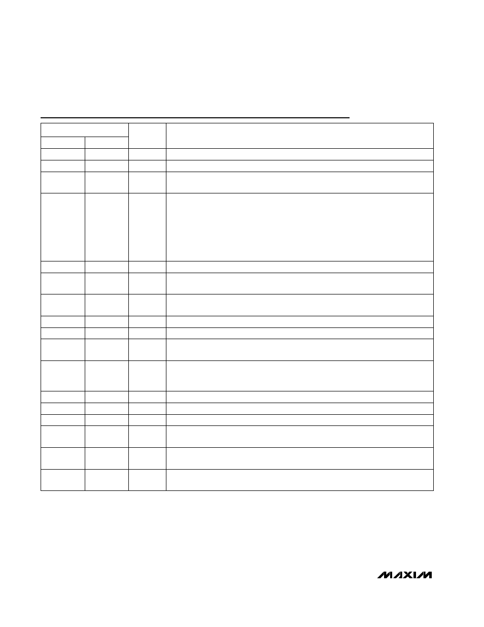
Pin Description
1
Low-Battery Comparator Non-Inverting Input
LBP
—
2
Low-Battery Comparator Inverting Input
LBN
—
3
Reference Output. Bypass with a 0.22µF capacitor to GND. REF can source up to
50µA.
REF
3
4
Switching-Mode Selection and External-Clock Synchronization Inputs.
• CLK/SEL=Low: Low-power, delivers up to 10% of full load current.
• CLK/SEL=High: High-power PWM mode. Full output power available. Operates in
low-noise, constant-frequency mode.
• CLK/SEL=External Clock: High-power PWM mode with the internal oscillator
synchronized to the external clock.
Turning on with CLK/SEL=0V also serves as a soft-start function since peak inductor
current is limited to 25% of that allowed in PWM mode.
CLK/SEL
4
5
Ground
GND
5
6
Power-Okay Comparator Output. Open drain N-channel output is low when V
OUT
is
10% below regulation point. No internal delay is provided.
POK
—
7
Shutdown Input. When ONB =high and ONA=low, the IC is off and the load is connect-
ed to the battery through the Schottky diode.
ONB
7
8
Turn ON Input. When ONA=high or ONB =low, the IC turns on.
ONA
8
9
Gain Block Output. This open-drain output sinks when V
AIN
REF . AO — 10 Gain Block AIN input. When AIN is low, AO sinks current. The transconductance from AIN — 11 DC-DC Converter Dual-Mode Feedback Input. For a fixed output voltage of +3.3V, FB 11 12 Source of N-Channel Power MOSFET Switch. Connect to high-current ground path. PGND 12 13 Drain of P-Channel Synchronous Rectifier and N-Channel Switch LX 13 14 Output Sense Input. Power source for the IC. OUT 14 15 Source of P-Channel Synchronous Rectifier MOSFET Switch. Connect an external POUT 15 16 Low-Battery Comparator Output. Open-drain N-channel output is low when LBN > LBP LBO — PIN MAX1701 MAX1700 FUNCTION NAME — Internal Connection. Leave open or connect to GND. I.C. 1, 2, 6, 9, 10, 16
AIN to AO is 9mmhos.
connect FB to GND. For adjustable output, connect a divider between POUT and GND
to set the output voltage in the range of 2.5V to 5V.
Schottky diode from LX to POUT.
Input hysteresis is 15mV.