Pin configurations (continued), Designing a pc board, Soft-start – Rainbow Electronics MAX1701 User Manual
Page 15: Intermittent supply/battery connections
low-noise power for DSP, control, and RF circuitry.
Typically, RF phones spend most of their life in standby
mode with only short periods in transmit/receive mode.
During standby, maximize battery life by setting
CLK/SEL = 0; this places the IC in low-power mode (for
the lowest quiescent power consumption).
Designing a PC Board
High switching frequencies and large peak currents
make PC board layout an important part of design.
Poor design can cause excessive EMI and ground-
bounce, both of which can cause instability or regula-
tion errors by corrupting the voltage and current
feedback signals.
Power components (such as the inductor, converter IC,
filter capacitors, and output diode) should be placed as
close together as possible, and their traces should be
kept short, direct, and wide. A separate low-noise
ground plane containing the reference and signal
grounds should only connect to the power-ground
plane at one point. This minimizes the effect of power-
ground currents on the part. Consult the MAX1701 EV
kit manual for a layout example.
On multilayer boards, do not connect the ground pins
of the power components using vias through an internal
ground plane. Instead, place them close together and
route them in a star-ground configuration using compo-
nent-side copper. Then use vias to connect the star
ground to the internal ground plane.
Keep the voltage feedback network very close to the
IC, within 0.2in. (5mm) of the FB pins. Keep noisy
traces, such as from the LX pin, away from the voltage
feedback networks. Separate them with grounded
copper. Consult the MAX1700 evaluation kit for a full
PC board example.
Soft-Start
To implement soft-start, set CLK/SEL low on power-up;
this forces low-power operation and reduces the peak
switching current to 550mA max. Once the circuit is in
regulation and start-up transients have settled,
CLK/SEL can be set high for full-power operation.
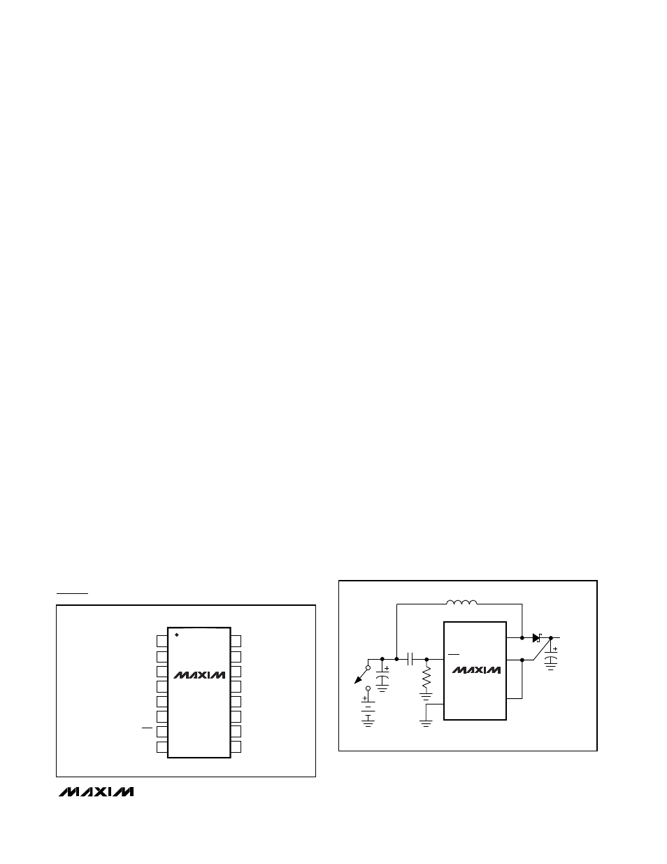
Intermittent Supply/Battery Connections
When boosting an input supply connected with a
mechanical switch, or a battery connected with spring
contacts, input power may sometimes be intermittent
as a result of contact bounce. When operating in PFM
mode with input voltages greater than 2.5V, restarting
after such dropouts may initiate high current pulses that
interfere with the MAX1700/MAX1701 internal MOSFET
switch control. If contact or switch bounce is anticipat-
ed in the design, use one of the following solutions.
1) Connect a capacitor (C
ONB
) from ONB to V
IN
, a 1M
Ω
resistor (R
ONB
) from ONB to GND, and tie ONA to GND
(Figure 12). This RC network differentiates fast input
edges at V
IN
and momentarily holds the IC off until V
IN
settles. The appropriate value of C
ONB
is 10
-5
times the
total output filter capacitance (C
OUT
), so a C
OUT
of
200µF results in C
ONB
= 2nF.
2) Use the system microcontroller to hold the
MAX1700/MAX1701 in shut down from the time when
power is applied (or reapplied) until the output capaci-
tance (C
OUT
) has charged to at least the input voltage.
Power-on reset times of tens of milliseconds accom-
plish this.
3) Ensure that the IC operates, or at least powers up, in
PWM mode (CLK/SEL = high). Activate PFM mode only
after the V
OUT
has settled and all of the system’s power-
on reset flags are cleared.
MAX1700/MAX1701
1-Cell to 3-Cell, High-Power (1A),
Low-Noise, Step-Up DC-DC Converters
______________________________________________________________________________________
15
16
15
14
13
12
11
10
9
1
2
3
4
5
6
7
8
LBP
LBO
POUT
OUT
LX
PGND
FB
AIN
AO
MAX1701
QSOP
LBN
REF
POK
CLK/SEL
GND
ONB
ONA
TOP VIEW
Pin Configurations (continued)
Figure 12. Connecting C
ONB
and R
ONB
when Switch or
Battery-Contact Bounce Is Anticipated
POUT
OUT
LX
13
14
15
8
7
C
OUT
200
µ
F
C
ONB
2nF
R
ONB
1M
ONA
ONB
MAX1700
MAX1701