Step-up converter – Rainbow Electronics MAX1701 User Manual
Page 10
MAX1700/MAX1701
Step-Up Converter
The step-up switching DC-DC converter generates an
adjustable output from 2.5V to 5.5V. During the first part
of each cycle, the internal N-channel MOSFET switch is
turned on. This allows current to ramp up in the induc-
tor and store energy in a magnetic field. During the
second part of each cycle, when the MOSFET is turned
off, the voltage across the inductor reverses and forces
current through the diode and synchronous rectifier to
the output filter capacitor and load. As the energy
stored in the inductor is depleted, the current ramps
down and the output diode and synchronous rectifier
turn off. Voltage across the load is regulated using
either low-noise PWM or low-power operation, depend-
ing on the CLK/SEL pin setting (Table 2).
Low-Noise PWM Operation
When CLK/SEL is pulled high, the MAX1700/MAX1701
operate in a higher power, low-noise pulse-width-
modulation (PWM) mode. During PWM operation, they
switch at a constant frequency (300kHz) and then mod-
ulate the MOSFET switch pulse width to control the
power transferred per cycle and regulate the voltage
across the load. In PWM mode the devices can output
up to 800mA. Switching harmonics generated by fixed-
frequency operation are consistent and easily filtered.
See the Noise Spectrum Plot in the
Typical Operating
Characteristics.
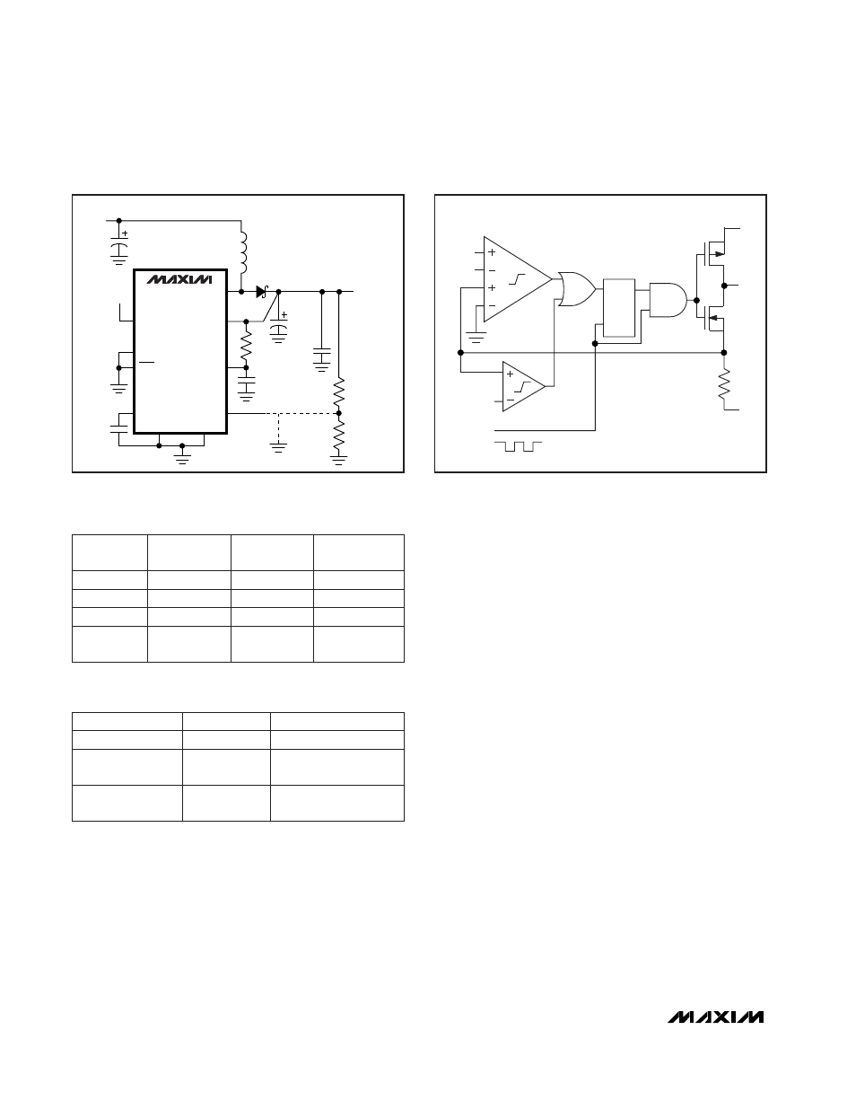
During PWM operation, each rising edge of the internal
clock sets a flip-flop, which turns on the N-channel
MOSFET switch (Figure 3). The switch is turned off
when the sum of the voltage-error, slope compensation,
and current-feedback signals trips a multi-input com-
parator and resets the flip-flop; the switch remains off
for the rest of the cycle. When a change occurs in the
output-voltage error signal into the comparator, it shifts
the level to which the inductor current is allowed to
ramp during each cycle and modulates the MOSFET
switch pulse width. A second comparator enforces an
inductor current limit of 1.6A max.
1-Cell to 3-Cell, High-Power (1A),
Low-Noise, Step-Up DC-DC Converters
10
______________________________________________________________________________________
PGND
GND
FB
POUT
OUT
LX
D1
OUTPUT
OUT
FIXED
OUTPUT
(GND)
MBR0520L
2 x
100
µ
F
ADJUSTABLE
L1
10
µ
H
REF
CLK/SEL
ONA
ONB
R2
R1
0.22
µ
F
0.22
µ
F
0.22
µ
F
22
µ
F
10
Ω
0.7V TO 5.5V
MAX1700
MAX1701
Figure 2. Fixed or Adjustable Output (PWM mode).
CLK/SEL
MODE
FEATURES
0
Low Power
Low supply current
1
PWM
Low noise,
high output current
External Clock
(200kHz to 400kHz)
Synchronized
PWM
Low noise,
high output current
Table 2. Selecting the Operating Mode
Table 1. Typical Available Output Current
POUT
LX
PGND
P
N
S
Q
R
FB
REF
1.3A CURRENT
LIMIT
OSC
Figure 3. Simplified PWM Controller Block Diagram
NUMBER
OF CELLS
INPUT
VOLTAGE (V)
OUTPUT
CURRENT (mA)
1 NiCd/NiMH
1.2
300
2 NiCd/NiMH
2.4
750
2 NiCd/NiMH
2.4
525
OUTPUT
VOLTAGE (V)
3.3
3.3
5.0
3 NiCd/NiMH
or 1 Li-Ion
3.6
850
5.0