Table 2. component manufacturers – Rainbow Electronics MAX1641 User Manual
Page 9
where V
TERM
= 2V and V
OUT
is the desired output
voltage.
Programming the Off-Time
When programming the off-time, consider such factors
as maximum inductor current ripple, maximum output
voltage, inductor value, and inductor current rating. The
output current ripple is less than the inductor current rip-
ple and depends heavily on the output capacitor’s size.
Perform the following steps to program the off-time:
1) Select the maximum output current ripple. I
R
(A)
2) Select the maximum output voltage. V
OUT
(MAX)(V)
3) Calculate the inductor value range as follows:
L
MIN
= (V
OUTMAX
x 1µs) / I
R
L
MAX
= (V
OUTMAX
x 10µs) / I
R
4) Select an inductor value in this range.
5) Calculate t
OFF
as follows:
6) Program t
OFF
by selecting R
TOFF
from:
R
TOFF
= (29.3 x 10
9
) x t
OFF
7) Calculate the switching frequency by:
fs = 1 / (t
ON
+ t
OFF
)
where t
ON
= (I
R
x L) / (V
IN
- V
OUT
) and I
R
= (V
OUT
x
t
OFF
) / L. L is the inductor value, V
IN
is the input volt-
age, V
OUT
is the output voltage, and I
R
is the output
peak-to-peak current ripple.
Note that R
TOFF
sets both the off-time and the pulse-
trickle charge period.
Reference
The on-chip reference is laser trimmed for a precise 2V
at REF. REF can source no more than 50µA. Bypass
REF with a 0.1µF capacitor to ground.
Constant-Current Loop: AC Loop
Compensation
The constant-current loop’s output is brought out at CC.
To reduce noise due to variations in switching currents,
bypass CC with a 1nF to 100nF capacitor to ground. A
large capacitor value maintains a constant average out-
put current but slows the loop response to changes in
switching current. A small capacitor value speeds up
the loop response to changes in switching current,
generating increased ripple at the output. Select C
CC
to optimize the ripple vs. loop response.
Synchronous Rectification
Synchronous rectification reduces conduction losses in
the rectifier by shunting the Schottky diode with a low-
resistance MOSFET switch. In turn, efficiency increases
by about 3% to 5% at heavy loads. To prevent cross-
conduction or “shoot-through,” the synchronous rectifier
turns on shortly after the P-channel power MOSFET
turns off. The synchronous rectifier remains off for 90%
of the off-time. In low-cost designs, the synchronous
rectifier FET may be replaced by a Schottky diode.
Component Selection
External Switching Transistors
The MAX1640/MAX1641 drive an enhancement-mode
P-channel MOSFET and a synchronous-rectifier N-
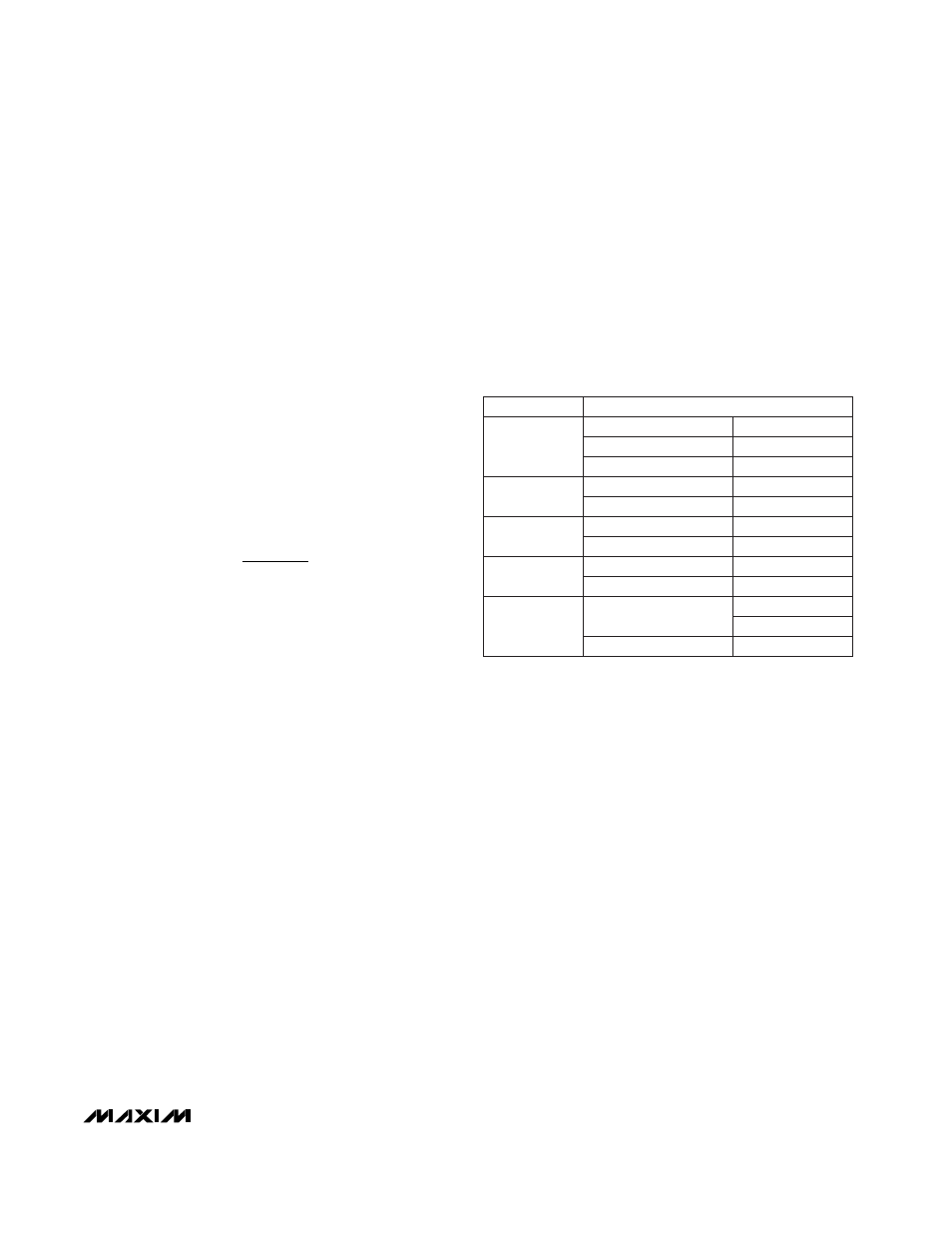
channel MOSFET (Table 2).
When selecting a P-channel FET, some important para-
meters to consider are on-resistance (r
DS(ON)
), maxi-
mum drain-to-source voltage (V
DS
max), maximum
gate-to-source voltage (V
GS
max), and minimum
threshold voltage (V
TH
min).
In high-current applications, MOSFET package power
dissipation often becomes a dominant design factor.
I2R power losses are the greatest heat contributor for
both high-side and low-side MOSFETs. Switching loss-
es affect the upper MOSFET only (P-channel), since the
Schottky rectifier or the N-FET body diode clamps the
switching node before the synchronous rectifier turns on.
Rectifier Diode
If an N-channel MOSFET synchronous rectifier is not
used, a Schottky rectifier is needed. The MAX1640/
t
=
L x I
V
OFF
R
OUTMAX
MAX1640/MAX1641
Adjustable-Output, Switch-Mode
Current Source with Synchronous Rectifier
_______________________________________________________________________________________
9
Table 2. Component Manufacturers
COMPONENT
MANUFACTURER
MOSFETs
Sense Resistor
Capacitors
International Rectifier
Dale
AVX
Sumida
Coilcraft
Inductor
Coiltronics
Siliconix
S14539DY
IRF7309
WSL-2010 series
TPS series
MBAR5340t3
CDRH125 series
D03316P series
UP2 series
IRC
LR2010-01 series
Sprague
595D series
Nihon
NSQ03A04
Rectifier
IN5817-IN5822
Motorola