Detailed description, Charge mode: programming the output currents – Rainbow Electronics MAX1641 User Manual
Page 7
MAX1640/MAX1641
Adjustable-Output, Switch-Mode
Current Source with Synchronous Rectifier
_______________________________________________________________________________________
7
_______________Detailed Description
The MAX1640/MAX1641 switch-mode current sources
utilize a hysteretic, current-mode, step-down pulse-
width-modulation (PWM) topology with constant off-
time. Internal comparators control the switching
mechanism. These comparators monitor the current
through a sense resistor (R
SENSE
) and the voltage at
TERM. When inductor current reaches the current limit
[(V
CS+
- V
CS-
) / R
SENSE
], the P-channel FET turns off
and the N-channel FET synchronous rectifier turns on.
Inductor energy is delivered to the load as the current
ramps down. This ramp rate depends on R
TOFF
and
inductor values. When off-time expires, the P-channel
FET turns back on and the N-channel FET turns off.
Two digital inputs, D0 and D1, select between four pos-
sible current levels (Table 1). In pulse-trickle mode, the
part operates for 12.5% of the period set by R
TOFF
,
resulting in a lower current for pulse-trickle charging.
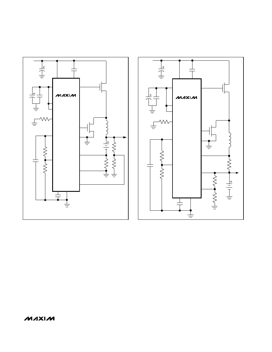
Figure 1 is the MAX1640/MAX1641 functional diagram.
Figure 2 shows the standard application circuits.
Charge Mode: Programming the
Output Currents
The sense resistor, R
SENSE
, sets two charging current
levels. Choose between these two levels by holding
D0 high, and toggling D1 either high or low (Table 1).
The fast-charge current level equals V
CS
/ R
SENSE
where V
CS
is the full-scale current-sense voltage of
150mV. Alternatively, calculate this current by V
REF
/
(13.3R
SENSE
). The top-off current equals V
SET
/
(13.3R
SENSE
). A resistor-divider from REF to GND pro-
grams the voltage at SET (Figure 3).
P
N
0.1
µ
F
4.7
µ
F
47
µ
F
0.33
µ
F
0.01
µ
F
0.1
µ
F
R1
R
TOFF
R2
SET
REF
TOFF
D1
D0
LDOL
PDRV
NDRV
PGND
CS+
CS-
TERM
GND
CC
R3
47
µ
H
V
OUT
BATT
1/2 IR7309
1/2 IR7309
R4
100m
Ω
LDOH
IN
MAX1641
P
N
0.1
µ
F
0.01
µ
F
4.7
µ
F
47
µ
F
0.33
µ
F
0.1
µ
F
R1
R2
SET
REF
TOFF
D1
D0
LDOL
PDRV
NDRV
PGND
CS+
CS-
R3
R4
TERM
GND
CC
47
µ
H
1/2 IR7309
1/2 IR7309
100m
Ω
BATT
V
OUT
R
TOFF
LDOH
IN
MAX1640
Figure 2a. Standard Application Circuit
Figure 2b. Standard Application Circuit