Typical operating characteristics (continued), Pin description – Rainbow Electronics MAX1641 User Manual
Page 5
MAX1640/MAX1641
Adjustable-Output, Switch-Mode
Current Source with Synchronous Rectifier
_______________________________________________________________________________________
5
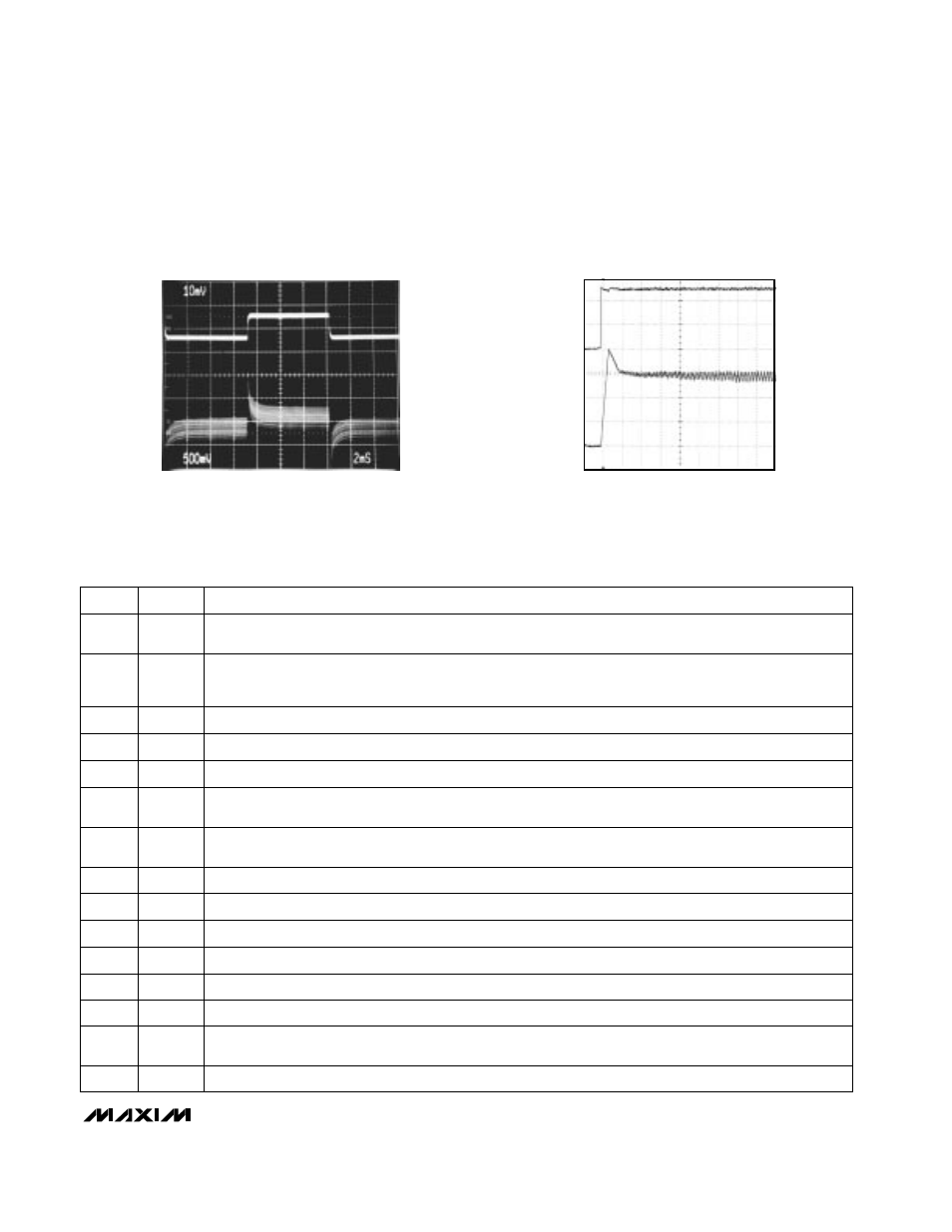
____________________________Typical Operating Characteristics (continued)
(Circuit of Figure 2, T
A
= +25°C, unless otherwise noted.)
A: OUTPUT CURRENT, D0 = D1 = 0 1A/div
V
IN
= 12V, V
SET
= 1V, R
LOAD
= 4
Ω,
NO OUTPUT CAPACITOR
B: LOAD VOLTAGE, AC coupled, 500mV/div
CURRENT-MODE CHANGE RESPONSE TIME
A
B
2ms/div
0A
0V
MAX1640/41 TOC 10
B
A
EXITING OFF MODE
MAX1640/41 TOC11
A: D0 = D1 = 1 2V/div
V
IN
= 12V, R
LOAD
= 4
Ω
B: OUTPUT CURRENT, 0.5A/div
20
µ
s/div
______________________________________________________________Pin Description
NAME
FUNCTION
1
LDOL
Internal, Ground-Referenced Low-Dropout Linear Regulator Output.
Bypass with a 0.1µF capacitor in parallel with a 4.7µF capacitor to GND.
2
TOFF
Off-Time Select Input. A resistor (R
TOFF
) connected from this pin to GND programs the off-time for the hys-
teretic PWM step-down converter. This resistor also sets the period in duty-cycle mode. See
Duty-Cycle
Mode and Programming the Off-Time.
PIN
3, 4
D1, D0
Digital Inputs. Select mode of operation (Table 1).
5
CC
Constant-Current Loop Compensation Input. Bypass with a 0.01µF capacitor to GND.
8
TERM
Maximum Output Voltage Termination Input. When V
TERM
exceeds the reference voltage, the comparator
resets the internal PWM latch, shutting off the external P-channel FET.
7
SET
Current Select Input. Program the desired current level by applying a voltage at SET between 0V and V
REF
,
(I = V
SET
/ 13.3R
SENSE
). See Figure 3.
6
REF
Reference Voltage Output (V
REF
= 2V). Bypass with a 0.1µF capacitor to GND.
13
NDRV
Gate Drive for an Optional N-Channel FET Synchronous Rectifier
12
PGND
High-Current Ground Return for the Output Drivers
11
CS+
Positive Current-Sense Comparator Input
10
CS-
Negative Current-Sense Comparator Input
9
GND
Ground
14
PDRV
Gate Drive for the P-Channel FET
15
LDOH
Internal, Input-Referenced Low-Dropout Linear Regulator Output.
Bypass with a 0.33µF capacitor to IN.
16
IN
Power-Supply Input. Input of the internal, low-dropout linear regulators.