Rainbow Electronics MAX1641 User Manual
Page 2
MAX1640/MAX1641
Adjustable-Output, Switch-Mode
Current Source with Synchronous Rectifier
2
_______________________________________________________________________________________
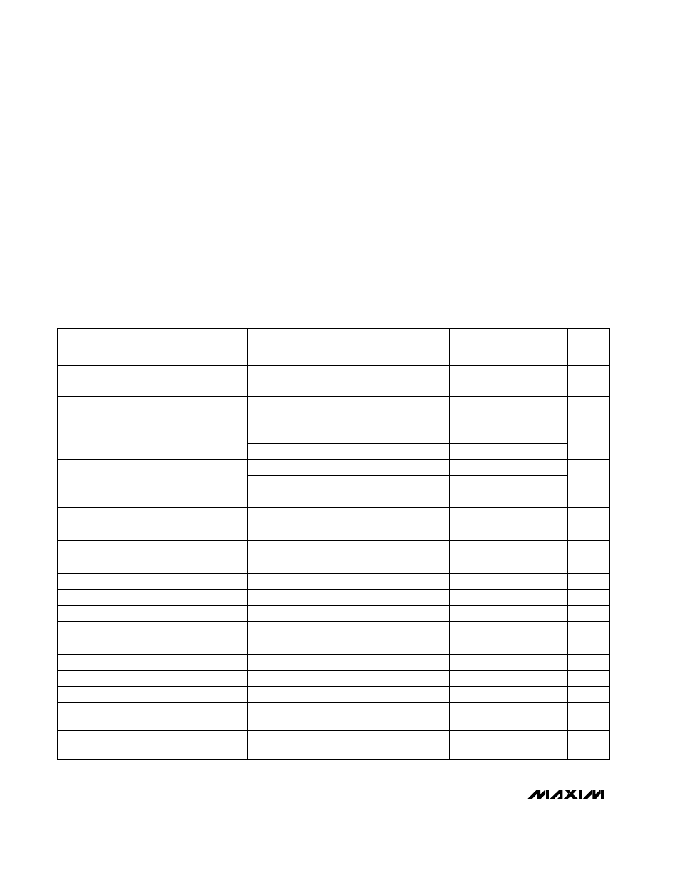
ABSOLUTE MAXIMUM RATINGS
ELECTRICAL CHARACTERISTICS
(V
IN
= +12V, V
OUT
= 6V, Circuit of Figure 2,
T
A
=
0°C to +85°C
, unless otherwise noted. Typical values are at T
A
= +25°C.)
Stresses beyond those listed under “Absolute Maximum Ratings” may cause permanent damage to the device. These are stress ratings only, and functional
operation of the device at these or any other conditions beyond those indicated in the operational sections of the specifications is not implied. Exposure to
absolute maximum rating conditions for extended periods may affect device reliability.
Note 1:
This ratio is generated by a 1:8 clock divider and is not an error source for current calculations.
IN to GND ...............................................................-0.3V to +28V
LDOH to IN ...............................................................+0.3V to -6V
LDOL to GND ...........................................................-0.3V to +6V
PDRV to GND .............................. (V
LDOH
- 0.3V) to (V
IN
+ 0.3V)
NDRV to GND .........................................-0.3V to (V
LDOL
+ 0.3V)
TOFF, REF, SET, TERM, CC to GND ......-0.3V to (V
LDOL
+ 0.3V)
D0, D1 to GND .........................................................-0.3V to +6V
CS+, CS- to GND ...................................................-0.3V to +28V
PGND to GND.....................................................................±0.3V
Continuous Power Dissipation (T
A
= +70°C)
QSOP (derate 8.30mW/°C above +70°C) ................... 667mW
Operating Temperature Range
MAX164_EEE ...................................................-40°C to +85°C
Storage Temperature Range .............................-65°C to +150°C
Lead Temperature (soldering, 10sec) ............................ +300°C
I
REF
= 0 to 50µA
D0 = D1 = low
D0 = D1 = low (off mode)
D0 or D1 = high
V
OUT
= 2V to 24V
V
IN
= V
OUT
+ 0.5V to 26V
MAX1641
MAX1641
MAX1640
V
IN
= 5.5V to 26V, I
LOAD
= 0 to 20mA
V
IN
= 5.5V to 26V, I
LOAD
= 0 to 20mA
MAX1640
CONDITIONS
µA
1
V
SET
Input Current
mV
4
10
Reference Load Regulation
V
1.96
2.00
2.04
V
REF
Reference Voltage
V
4.05
4.20
4.35
V
LDOL
Undervoltage Lockout
µA
1
Output Current in Off Mode
500
mA
2
4
Quiescent V
IN
Supply Current
0.1
%/V
0.1
0.4
Output Current Compliance
%/V
0.03
Current-Sense Line Regulation
34
37.5
41
mV
36
42
48
147
150
153
mV
142
150
158
Full-Scale Current-Sense
Threshold
V
V
IN
-
V
IN
-
V
IN
-
5.5
5.0
4.5
V
LDOH
Linear-Regulator Output
Voltage, V
IN
Referenced
V
4.5
5.0
5.5
V
LDOL
Linear-Regulator Output
Voltage, Ground Referenced
UNITS
MIN
TYP
MAX
SYMBOL
PARAMETER
V
5.5
26
V
IN
Input Voltage Range
FET Drive Output Resistance
PFET and NFET drive
12
Ω
Off-Time Range
1
10
µs
Off-Time Accuracy
R
TOFF
= 62k
Ω
1.7
2.2
2.7
µs
Pulse-Trickle Mode Duty-Cycle
Period
D0 = low, D1 = high, R
TOFF
= 100k
Ω
27
33
40
ms
Pulse-Trickle Mode Duty Cycle
(Note 1)
D0 = low, D1 = high, R
TOFF
= 100k
Ω
12.5
%
Quarter-Scale Current-Sense
Threshold
MAX1640
MAX1641
µA