Max500 cmos, quad, serial-interface 8-bit dac, Applications information, Power-supply and reference operating ranges – Rainbow Electronics MAX500 User Manual
Page 9: Ground management

The SRO output swings from V
DD
to DGND. Cascading
to other MAX500s poses no problem. If SRO is used to
drive a TTL-compatible input, use a clamp diode
between TTL +5V and V
DD
and the current-limiting
resistor to prevent potential latchup problems with
the 5V supply.
Table 2 shows the truth table for SDA, SCL,
LOAD, and
LDAC operation. Figures 5 and 6 show the timing dia-
grams for the MAX500.
__________Applications Information
Power-Supply and Reference
Operating Ranges
The MAX500 is fully specified to operate with V
DD
between +12V ±5% and +15V ±10% (+11.4V to
+16.5V), and with V
SS
from 0V to -5.5V. 8-bit perfor-
mance is also guaranteed for single-supply operation
(V
SS
= 0V), however, zero-code error is reduced when
V
SS
is -5V (see
Output Buffer Amplifiers
section).
For an adequate DAC and buffer operating range, the
V
REF
voltage must always be at least 4V below V
DD
.
The MAX500 is specified to operate with a reference
input range of +2V to V
DD
- 4V.
Ground Management
Digital or AC transient signals between AGND and
DGND will create noise at the analog outputs. It is rec-
ommended that AGND and DGND be tied together at
the DAC and that this point be tied to the highest quali-
ty ground available. If separate ground buses are used,
then two clamp diodes (1N914 or equivalent) should be
connected between AGND and DGND to keep the two
ground buses within one diode drop of each other. To
avoid parasitic device turn-on, AGND must not be
allowed to be more negative than DGND. DGND should
be used as supply ground for bypassing purposes.
MAX500
CMOS, Quad, Serial-Interface
8-Bit DAC
_______________________________________________________________________________________
9
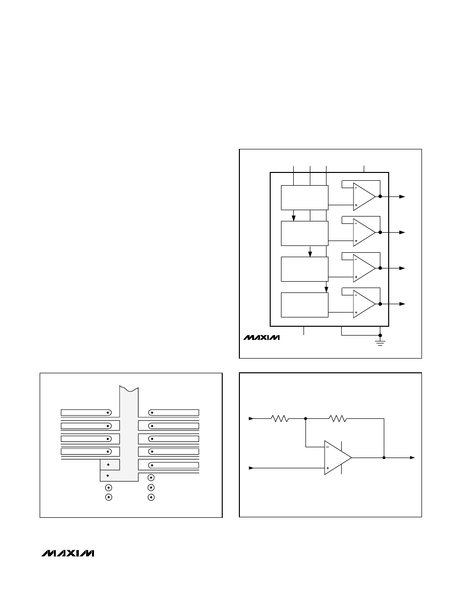
Figure 7. Suggested MAX500 PC Board Layout for
Minimizing Crosstalk
Figure 8. MAX500 Unipolar Output Circuit
COMPONENT SIDE (TOP VIEW)
V
OUT
C
V
OUT
D
V
DD
V
REF
C
V
REF
D
SYSTEM GND
V
OUT
B
V
OUT
A
V
SS
V
REF
A/B
AGND
DGND
V
REF
D
DAC A
DAC B
DAC C
DAC D
V
REF
C
V
REF
A/B
MAX500
V
OUT
A
V
OUT
B
V
OUT
C
V
OUT
D
DIGITAL
INPUTS
NOT
SHOWN
REFERENCE INPUTS
2
1
16
15
V
DD
+15V
13
12
4
14
3
-5V (OR GND)
5
6
V
SS
AGND
DGND
V
REF
DAC
OUTPUT
FROM MAX500
R1
R2
+15V
-15V
R1 = R2 = 10k
Ω
±0.1%
NOTE: V
REF
IS THE REFERENCE INPUT FOR THE MAX500
V
OUT
Figure 9. Bipolar Output Circuit
