Max500 cmos, quad, serial-interface, 8-bit dac, Chip topography ____pin configurations (continued) – Rainbow Electronics MAX500 User Manual
Page 12
Maxim cannot assume responsibility for use of any circuitry other than circuitry entirely embodied in a Maxim product. No circuit patent licenses are
implied. Maxim reserves the right to change the circuitry and specifications without notice at any time.
12
__________________Maxim Integrated Products, 120 San Gabriel Drive, Sunnyvale, CA 94086 (408) 737-7600
© 1996 Maxim Integrated Products
Printed USA
is a registered trademark of Maxim Integrated Products.
MAX500
CMOS, Quad, Serial-Interface,
8-Bit DAC
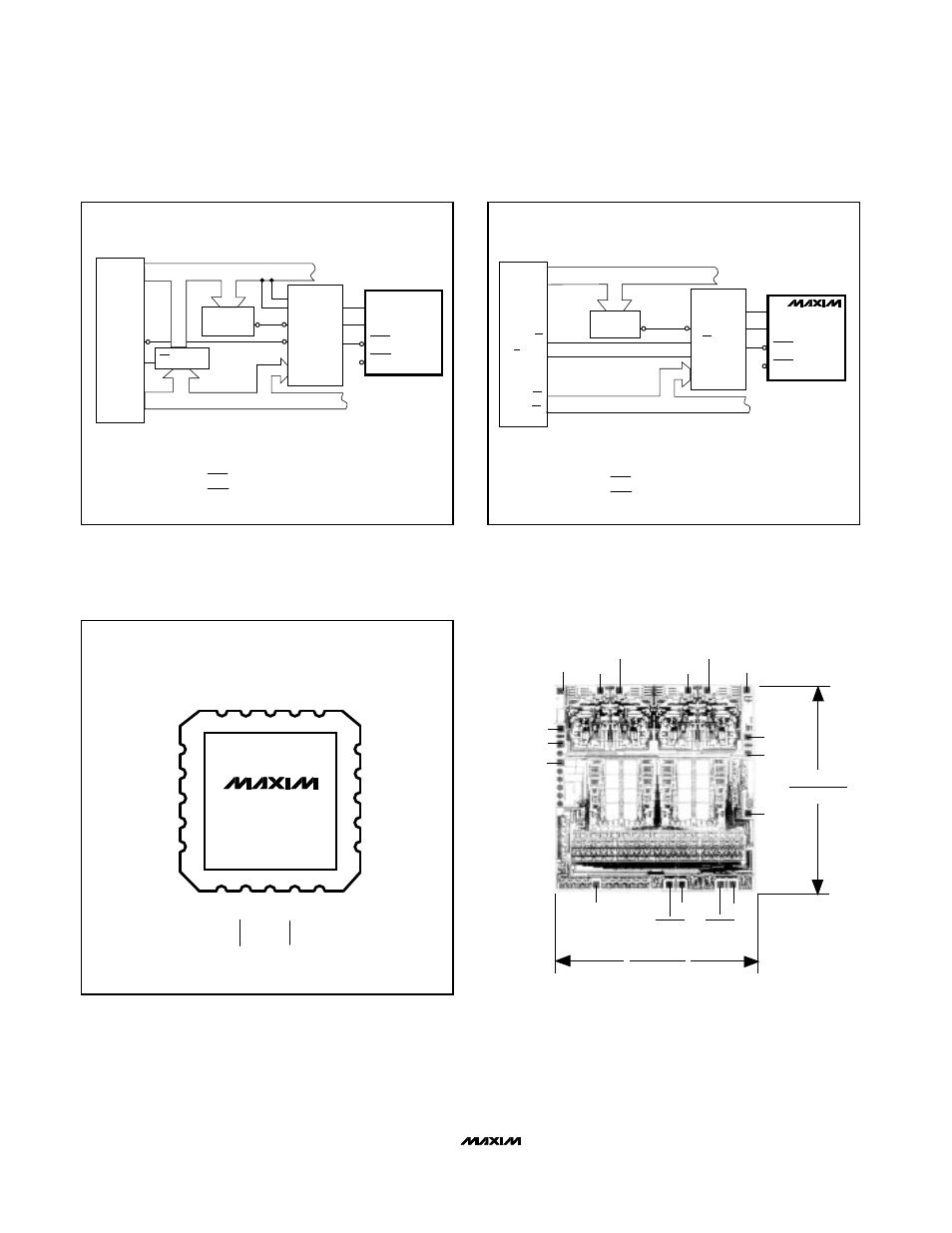
___________________Chip Topography
____Pin Configurations (continued)
CONNECT LOAD TO P1.3 FOR 3-WIRE MODE OR
CONNECT LOAD TO V
DD
FOR 2-WIRE MODE
*
A15
A8
8085/
8088
WR
ALE
AD7
AD0
EN LATCH
ADDRESS BUS
ADDRESS
DECODE
ADDRESS AND DATA BUS
A0
CS
WR
D7
D0
SCL
SDA
LDAC
LOAD*
82C55
PA0
PA1
PA2
PA3
MAX500
. .
A1
CONNECT LOAD TO P1.3 FOR 3-WIRE MODE OR
CONNECT LOAD TO V
DD
FOR 2-WIRE MODE
*
A15
A0
6809/
6502
R/W
Θ
OR E
∆
7
D0
ADDRESS BUS
ADDRESS
DECODE
DATA BUS
C32
R/W
DB7
DB0
6821
6521 PA0
PA1
PA2
PA3 . .
E
SCL
SDA
LDAC
LOAD*
MAX500
Figure 15. 8085/8088 with Programmable Peripheral Interface
Figure 16. 6809/6502 Interface
V
REF
C
SRO
V
REF
D
V
REF
B
AGND
V
REF
A
Vss V
OUT
A
V
OUT
B
V
DD
SCL
LOAD
LDAC
DGND
SDA
0.159"
(4.039mm)
0.150"
(3.810mm)
V
OUT
C
V
OUT
D
14
15
16
17
18
4
5
6
7
8
3
2
1
20
19
9
10
11
12
13
MAX500
V
SS
V
REF
A/B
AGND
N.C.
N.C.
V
DD
V
REF
C
V
REF
D
SRO
N.C.
V
OUT
A
V
OUT
B
N.C.
V
OUT
C
V
OUT
D
DGND
LDAC
SDA
LOAD
SCL
LCC
TOP VIEW