Max500, Cmos, quad, serial-interface 8-bit dac, Digital inputs and interface logic – Rainbow Electronics MAX500 User Manual
Page 6: Wire interface
MAX500
sink, as well as source up to 5mA. This is especially
important in single-supply applications, where V
SS
is
connected to AGND, so that the zero error is kept at or
under 1/2LSB (V
REF
= +10V). A plot of the Output Sink
Current vs. Output Voltage is shown in the
Typical
Operating Characteristics
section.
Digital Inputs
and Interface Logic
The digital inputs are compatible with both TTL and 5V
CMOS logic; however, the power-supply current (I
DD
)
is somewhat dependent on the input logic level. Supply
current is specified for TTL input levels (worst case) but
is reduced (by about 150µA) when the logic inputs are
driven near DGND or 4V above DGND.
Do not drive the digital inputs directly from CMOS logic
running from a power supply exceeding 5V. When driv-
ing SCL through an opto-isolator, use a Schmitt trigger
to ensure fast SCL rise and fall times.
The MAX500 allows the user to choose between a
3-wire serial interface and a 2-wire serial interface.
The choice between the 2-wire and the 3-wire inter-
face is set by the
LOAD signal. If the LOAD is allowed
to float (it has a weak internal pull-up resistor to V
DD
),
the 2-wire interface is selected. If the
LOAD signal is
kept to a TTL-logic high level, the 3-wire interface
is selected.
3-Wire Interface
The 3-wire interface uses the classic Serial Data (SDA),
Serial Clock (SCL), and
LOAD signals that are used
in standard shift registers. The data is clocked in on
the falling edge of SCL until all 10 bits (8 data bits and
2 address bits) are entered into the shift register.
CMOS, Quad, Serial-Interface
8-Bit DAC
6
_______________________________________________________________________________________
INPUT
(5V/div)
OUTPUT
(20mV/div)
DYNAMIC RESPONSE
(V
SS
= -5V or 0V)
2
µ
s/div
LDAC
5V/div
OUTPUT
5V/div
V
SS
V
DD
PMOS
(+)
FROM
INVERTED
DAC
OUTPUT
INPUTS
C
C
(-)
NPN
EMITTER
FOLLOWER
PULL-UP
V
OUT
NMOS
ACTIVE
PULL-DOWN
CIRCUIT
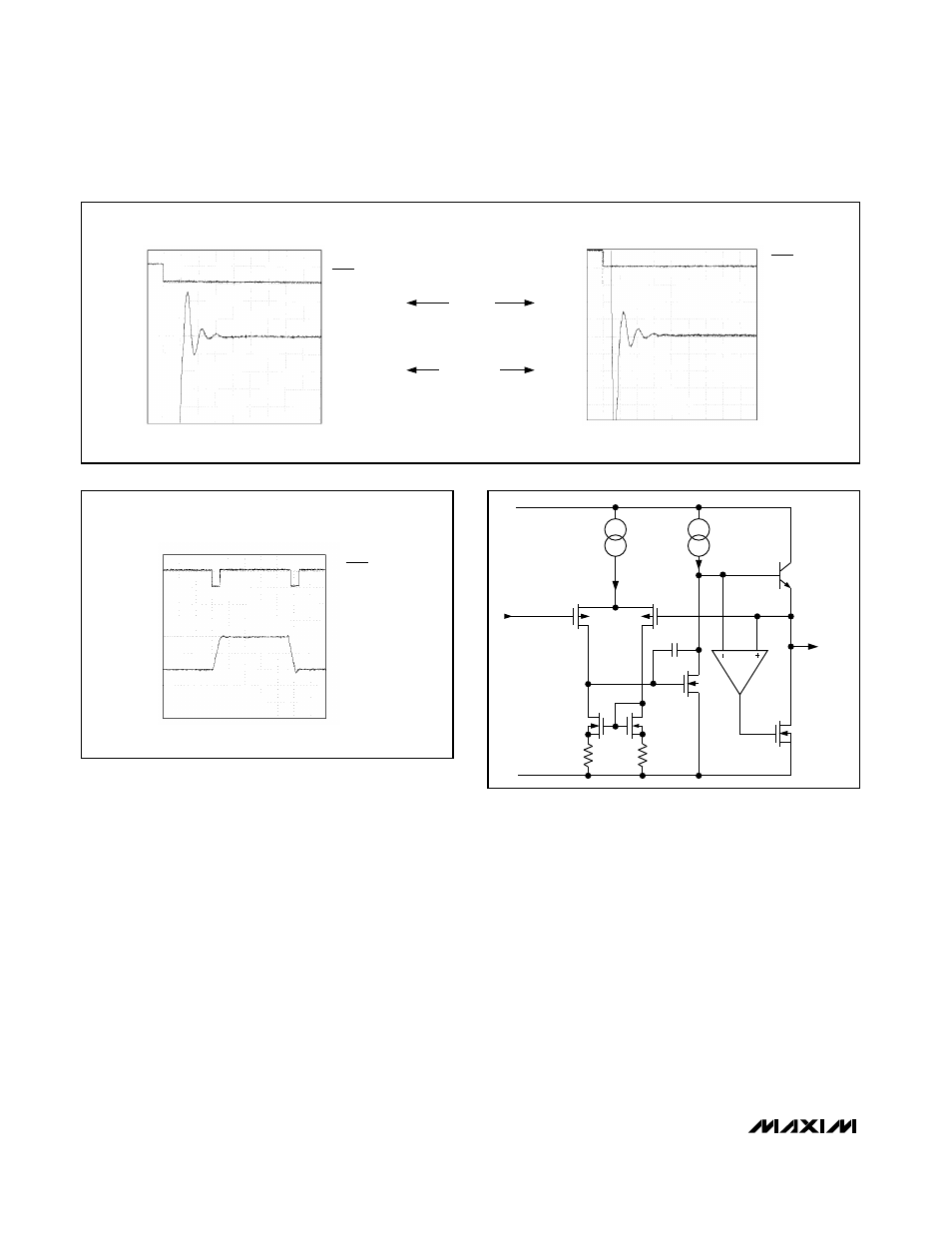
Figure 2. Positive and Negative Settling Times
Figure 3. Dynamic Response
Figure 4. Simplified Output Buffer Circuit
POSITIVE STEP
(V
SS
= -5V or 0V)
1
µ
s/div
LDAC
5V/div
OUTPUT
100mV/div
NEGATIVE STEP
(V
SS
= -5V or 0V)
1
µ
s/div
LDAC
5V/div
OUTPUT
100mV/div