Max500, Cmos, quad, serial-interface 8-bit dac – Rainbow Electronics MAX500 User Manual
Page 10
MAX500
Careful PC board ground layout techniques should be
used to minimize crosstalk between DAC outputs, the
reference input(s), and the digital inputs. This is partic-
ularly important if the reference is driven from an AC
source. Figure 7 shows suggested PC board layouts for
minimizing crosstalk.
Unipolar Output
In unipolar operation, the output voltages and the refer-
ence input(s) are the same polarity. The unipolar circuit
configuration is shown in Figure 8 for the MAX500. The
device can be operated from a single supply with a
slight increase in zero error (see
Output Buffer
Amplifiers
section). To avoid parasitic device turn-on,
the voltage at V
REF
must always be positive with
respect to AGND. The unipolar code table is given in
Table 3.
Bipolar Output
Each DAC output may be configured for bipolar opera-
tion using the circuit in Figure 9. One op amp and two
resistors are required per channel. With R1 = R2:
V
OUT
= V
REF
(2D
A
- 1)
where D
A
is a fractional representation of the digital
word in Register A.
Table 4 shows the digital code versus output voltage
for the circuit in Figure 9.
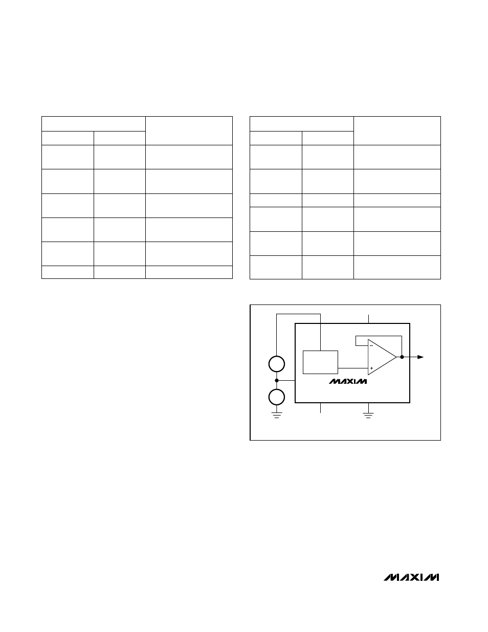
Offsetting AGND
AGND can be biased above DGND to provide an arbi-
trary nonzero output voltage for a “zero” input code. This
is shown in Figure 10. The output voltage at V
OUT
A is:
V
OUT
A = V
BIAS
+ D
A
V
IN
where D
A
is a fractional representation of the digital
input word. Since AGND is common to all four DACs,
all outputs will be offset by V
BIAS
in the same manner.
Since AGND current is a function of the four DAC
codes, it should be driven by a low-impedance source.
V
BIAS
must be positive.
CMOS, Quad, Serial-Interface
8-Bit DAC
10
______________________________________________________________________________________
DAC A
MAX500
4
14
AGND
2
V
OUT
A
DGND
V
SS
V
REF
A/B
V
DD
3
6
+
V
IN
-
+
V
BIAS
-
5
+15V
-5V (OR GND)
DIGITAL INPUTS NOT SHOWN
Figure 10. AGND Bias Circuit
Table 3. Unipolar Code Table
Table 4. Bipolar Code Table
1 0 0 0
DAC CONTENTS
0 0 0 1
MSB
LSB
ANALOG
OUTPUT
1 1 1 1
1 1 1 1
127
+V
REF
(
––––
)
128
1
+V
REF
(
––––
)
128
1 0 0 0
0 0 0 0
0V
0 1 1 1
1 1 1 1
1
-V
REF
(
––––
)
128
0 0 0 0
0 0 0 0
128
-V
REF
(
––––
)
= -V
REF
128
0 0 0 0
0 0 0 1
127
-V
REF
(
––––
)
128
1 0 0 0
DAC CONTENTS
0 0 0 1
MSB
LSB
ANALOG
OUTPUT
1 1 1 1
1 1 1 1
255
+V
REF
(
––––
)
256
129
+V
REF
(
––––
)
256
1 0 0 0
0 0 0 0
128 V
REF
+V
REF
(
––––
)
= +
––––
256 2
0 1 1 1
1 1 1 1
127
+V
REF
(
––––
)
256
0 0 0 0
0 0 0 0
0V
0 0 0 0
0 0 0 1
1
+V
REF
(
––––
)
256
1
Note:
1LSB = (V
REF
) (2
-8
) = +V
REF
(
–––
)
256
1
Note:
1LSB = (V
REF
) (2
-8
) = +V
REF
(
–––
)
256