Max500 cmos, quad, serial-interface 8-bit dac, Using an ac reference, Generating v – Rainbow Electronics MAX500 User Manual
Page 11: Digital interface applications
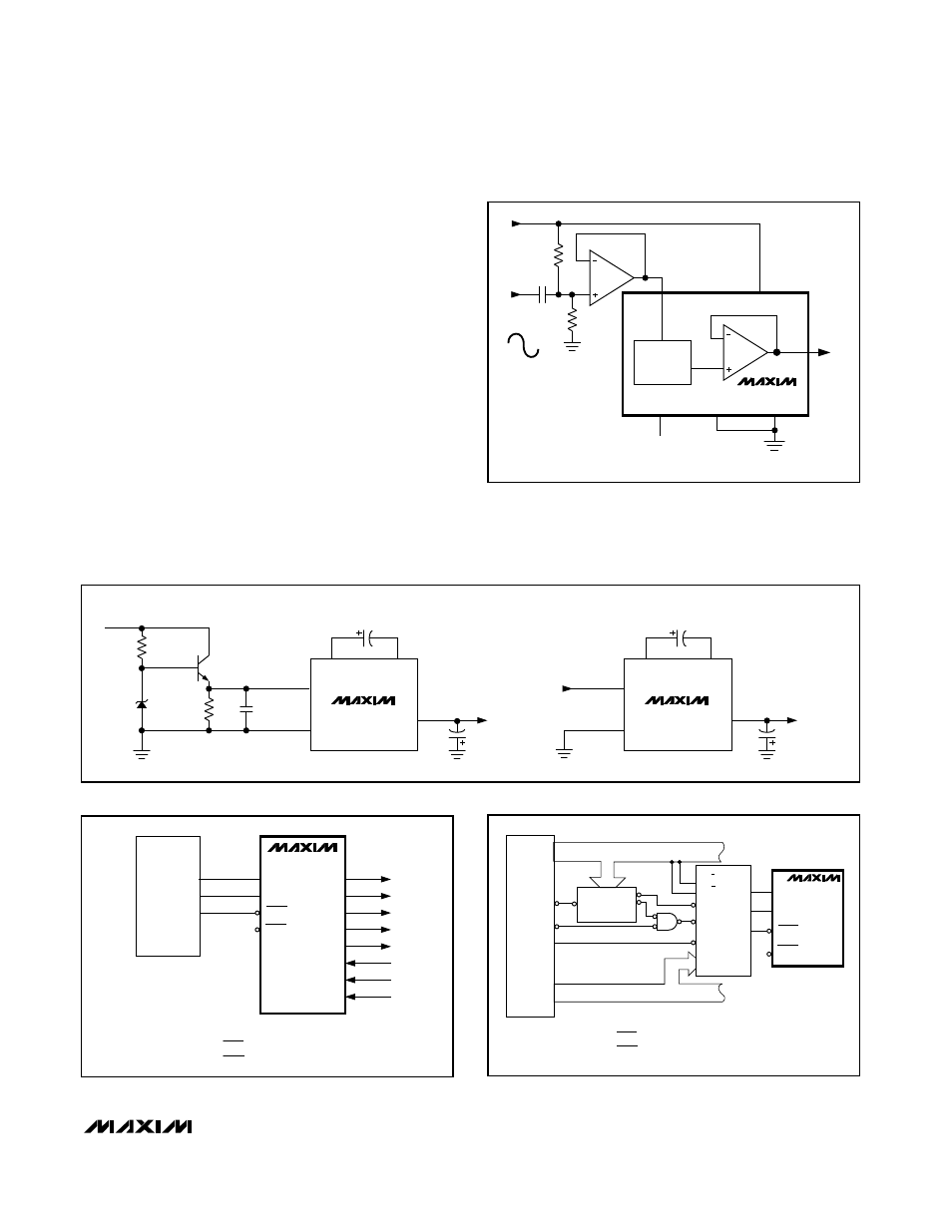
Using an AC Reference
In applications where V
REF
has AC signal components,
the MAX500 has multiplying capability within the limits
of the V
REF
input range specifications. Figure 11 shows
a technique for applying a sine-wave signal to the refer-
ence input, where the AC signal is biased up before
being applied to V
REF
. Output distortion is typically less
than 0.1% with input frequencies up to 50kHz, and the
typical -3dB frequency is 700kHz. Note that V
REF
must
never be more negative than AGND.
Generating V
SS
The performance of the MAX500 is specified for both
dual and single-supply (V
SS
= 0V) operation. When the
improved performance of dual-supply operation is
desired, but only a single supply is available, a -5V V
SS
supply can be generated using an ICL7660 in one of
the circuits of Figure 12.
Digital Interface Applications
Figures 13 through 16 show examples of interfacing the
MAX500 to most popular microprocessors.
MAX500
CMOS, Quad, Serial-Interface
8-Bit DAC
______________________________________________________________________________________
11
DAC B
MAX500
4
14
1 V
OUT
B
DGND
V
SS
V
REF
A/B
V
DD
3
6
-5V (OR GND)
DIGITAL INPUTS NOT SHOWN
AGND
V
OUT
B
+4V
-4V
AC
REFERENCE
INPUT
+15V
15k
10k
5
ICL7660
CAP+
CAP-
V+
GND
V
OUT
ICL7660
CAP+
CAP-
V+
GND
V
OUT
6V
ZENER
12V to 15V
10k
2N2222
10k
10
µ
F
8
3
2
10
µ
F
4
5
-5V
V
SS
OUT
10
µ
F
+5V
LOGIC
SUPPLY
-5V
V
SS
OUT
10
µ
F
8
3
4
5
10
µ
F
2
SCL
SDA
LDAC
LOAD*
80C51
P1.0
P1.1
P1.2
P1.3
CONNECT LOAD TO P1.3 FOR 3-WIRE MODE OR
CONNECT LOAD TO V
DD
FOR 2-WIRE MODE
. . . . . . .
SRO
V
OUT
A
V
OUT
B
V
OUT
C
V
OUT
D
V
REF
A/B
V
REF
C
V
REF
D
MAX500
*
ADDRESS BUS
EN ADDRESS
CODE
B/A
DATA BUS
CONNECT LOAD TO P1.3 FOR 3-WIRE MODE OR
CONNECT LOAD TO V
DD
FOR 2-WIRE MODE
C/D
CE
RD
INT
D7
D0
Z8420
B0
B1
B2
B3
A15
A0
Z80
I/O REQ
WR
INT
D7
D0
A1
A0
SCL
SDA
LDAC
LOAD*
. .
MAX500
*
Figure 11. AC Reference Input Circuit
Figure 12. Generating -5V for V
SS
Figure 14. Z-80 with Z8420 PIO Interface
Figure 13. 80C51 Interface