Max500, Cmos, quad, serial-interface 8-bit dac – Rainbow Electronics MAX500 User Manual
Page 8
MAX500
A low level on
LOAD line initiates the transfer of data
from the shift register to the addressed input register.
The data can stay in this register until all four of the
input registers are updated. Then all of the DAC regis-
ters can be simultaneously updated using the
LDAC
(load DAC) signal. When
LDAC is low, the input regis-
ter’s data is loaded into the DAC registers (see Figure 5
for timing diagram). This mode is cascadable by con-
necting Serial Output (SRO) to the second chip’s SDA
pin. The delay of the SRO pin from SCL does not cause
setup/hold time violations, no matter how many
MAX500s are cascaded. Restrict the voltage at
LDAC
and
LOAD to +5.5V for a logic high.
2-Wire Interface
The 2-wire interface uses SDA and SCL only.
LOAD
must be floating or tied to V
DD
. Each data frame (8 data
bits and 2 address bits) is synchronized by a timing
relationship between SDA and SCL (see Figure 6 for
the timing diagram). Both SDA and SCL should normal-
ly be high when inactive. A falling edge of SDA (while
SCL is high) followed by a falling edge of SCL (while
SDA is low) is the start condition. This always loads a 0
into the first bit of the shift register. The shift register is
extended to 11 bits so this “data” will not affect the
input register information. The timing now follows the 3-
wire interface, except the SDA line is not allowed to
change when SCL is high (this prevents the MAX500
from retriggering its start condition). After the last data
bit is entered, the SDA line should go low (while the
SCL line is low), then the SCL line should rise followed
by the SDA line rising. This is defined as the stop con-
dition, or end of frame.
Cascading the 2-wire interface can be done, but the
user must be careful of both timing and formatting.
Timing must take into account the intrinsic delay of the
SRO pin from the internally generated start/stop condi-
tions. The t
S2
value should be increased by n times t
D1
(where n = number of cascaded MAX500s). The t
LDS
value should also be increased by n times t
D1
. No other
timing parameters need to be modified. A more serious
concern is one of formatting. Generally, since each
frame has a start/stop condition, each chip that has
data cascaded through it will accept that data as if it
were its own data. Therefore, to circumvent this limita-
tion, the user should not generate a stop bit until all
DACs have been loaded. For example, if there are
three MAX500s cascaded in the 2-wire mode, the data
transfer should begin with a start condition, followed by
10 data bits, a zero bit, 10 data bits, a zero bit, 10 data
bits, and then a stop condition. This will prevent each
MAX500 from decoding the middle data for itself.
The data is entered into the shift register in the follow-
ing order:
A1 A0 D7 D6 D5 D4 D3 D2 D1 D0
(First) (MSB) (Last)
where address bits A1 and A0 select which DAC regis-
ter receives data from the internal shift register. Table 1
lists the channel addresses. D7 (MSB) through D0 is
the data byte.
Since
LDAC is asynchronous with respect to SCL, SDA,
and
LOAD, care must be taken to assure that incorrect
data is not latched through to the DAC registers. If the
3-wire serial interface is used,
LDAC can be either tied
low permanently or tied to
LOAD as long as t
LDS
is
always maintained. However, if the 2-wire interface is
used,
LDAC should not fall before the stop condition is
internally detected. (This is the reason for the t
LDS
delay of
LDAC after the last rising edge of SDA.)
CMOS, Quad, Serial-Interface
8-Bit DAC
8
_______________________________________________________________________________________
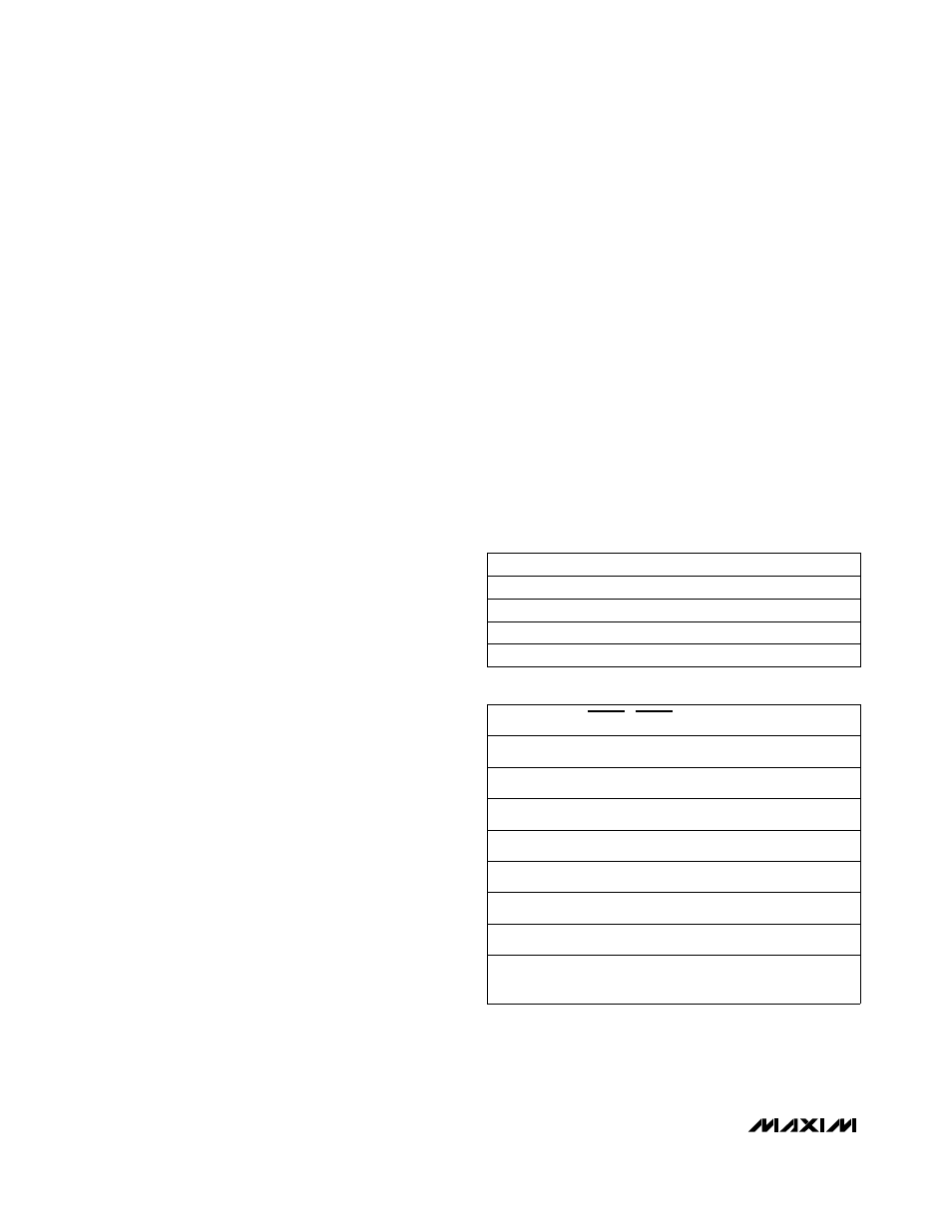
A1
A0
SELECTED INPUT REGISTER
L
L
DAC A Input Register
L
H
DAC B Input Register
H
L
DAC C Input Register
H
H
DAC D Input Register
SCL
SDA
LOAD LDAC
FUNCTION
F
Data
V
DD
H
Latching data into
shift register (2W)
H
Data
V
DD
H
Data should not be
changing (2W)
L
X
V
DD
H
Data is allowed to
change (2W)
F
Data
M
H
Latching data into
shift register (3W)
H
X
M
H
Data is allowed to
change (3W)
L
X
M
H
Data is allowed to
change (3W)
H
X
L
H
Loads input register
from shift register (3W)
H
X
L
L
DAC register reflects
data held in their respective
input registers
Notes:
H = Logic High
2W = 2-Wire
L = Logic Low
3W = 3-Wire
M = TTL Logic High
F = Falling Edge
X = Don’t Care
Table 1. DAC Addressing
Table 2. Logic Input Truth Table