Pin description – Rainbow Electronics MAX769 User Manual
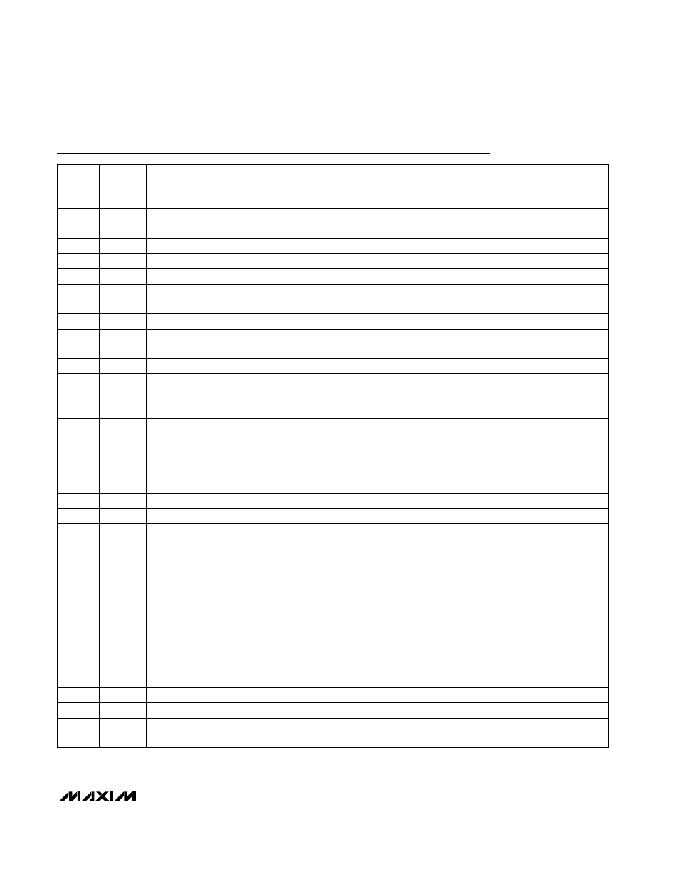
Page 7
MAX769
2 or 3-Cell, Step-Up/Down,
Two-Way Pager System IC
_______________________________________________________________________________________
7
Pin Description
25
OUT
DC-DC Converter Output and Feedback Point. Digitally controlled from 1.8V to 4.9V in 100mV steps
(Table 5).
27
CS
Chip Select for SPI Serial Interface
28
LX2
Connect LX2 to the other inductor terminal. LX2 is internally connected to an NFET that switches to PGND
and a PFET that switches to BATT.
26
BATT
Positive Connection to Battery. The IC is powered from OUT.
24
REG1
PFET Output Connected to OUT. Output is clamped such that it cannot rise above 3.3V, regardless of the
voltage set at OUT.
20
REG3
1V, 2mA Regulator Output. On via the serial interface. Low noise.
22
R2IN
REG2 Input. Connect to OUT, REG1, or another voltage source.
23
NICD
15mA or 1mA Settable Charge Current from OUT to 3-Cell NiCd Stack. When the NICD_REG_ON bit is set
(Table 1), NICD becomes an input to the linear regulator at OUT, and the DC-DC converter is off.
21
REG2
24mA REG2 Output. Linearly regulated to the voltage at the OFS pin (voltage difference = 10µA x R
OFS
).
REG2 isolates noise.
18
DR2IN
Logic Input. ANDed with the DR2ON bit to control the DR2 switch.
19
DR2
Open-Drain FET Switch. On via AND of the DR2ON bit and the DR2IN pin.
17
DR1
Open-Drain FET Switch. Activated via the serial-interface bit.
9
CH0
CH0 is compared to a 7-bit DAC that adjusts from 0.2V to 1.27V. The comparison result is sent to the CH0
OUT register.
13
SYNC
Sync Input for PWM Switch Rate. A 38.4kHz input results in a 268.8kHz PWM rate (seven times the SYNC
frequency).
15
AGND
Analog Ground
16
DRGND
Ground for DR1 and DR2 FET Sources
14
OFS
Resistor sets offset between OUT (or REG1 or any other point) and REG2. R
OFS
= 15k
Ω
results in 150mV.
11
LBI
Low-Battery Input. Triggers LBO and internal serial bit.
12
FILT
An external RC network sets the PLL loop response to adjust frequency lock time versus jitter: 1nF
||
(22nF +
10k
Ω
).
10
RSIN
Reset Input. Triggers RSO and resets IC when input is below 0.6V. Comparator with hysteresis (18mV).
5
SCL
Serial Clock for SPI Interface
7
RSO
Reset Output. Open drain goes low when RSIN drops below 0.6V. All serial registers are reset (or set) to
POR state as well.
8
REF
1.28V Reference. Bypass with a 1µF capacitor.
6
LBO
Open-Drain Output for LBI Comparator
3
SDO
Serial Data Output for SPI Interface
4
PGND
Power Ground. Source of LX1 and LX2 NFETs.
2
SDI
Serial Data Input for SPI Interface
NAME
FUNCTION
1
LX1
Connect LX1 to the inductor. LX1 is internally connected to an NFET that switches to PGND and a PFET that
switches to OUT.
PIN