Rainbow Electronics MAX769 User Manual
Page 14
MAX769
2 or 3-Cell, Step-Up/Down,
Two-Way Pager System IC
14
______________________________________________________________________________________
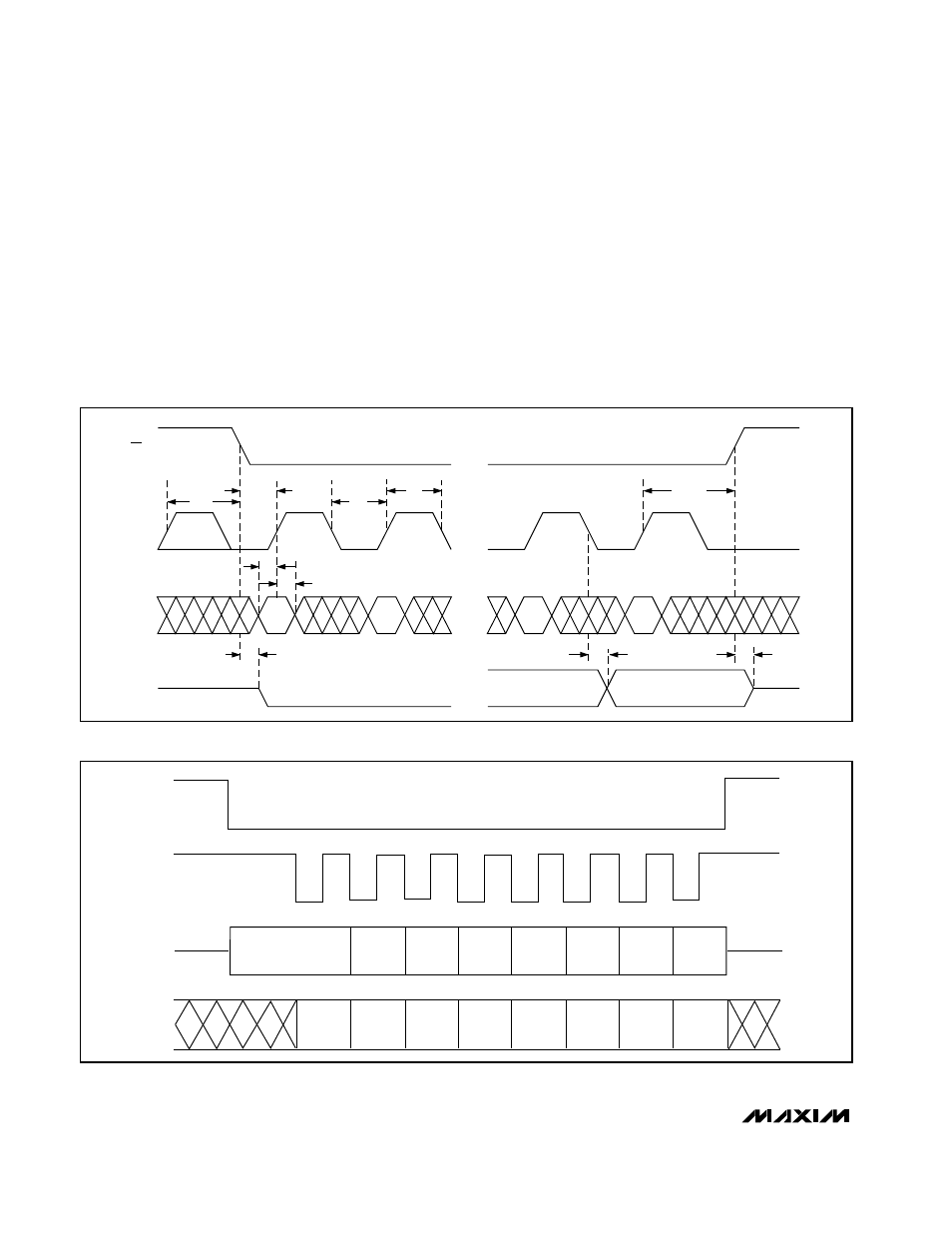
Serial data is clocked in and out MSB first. Input data is
latched on the CLK rising edge, and output data is
shifted out on the CLK falling edge. When CS goes low,
DO immediately contains the MSB output bit (D7). D6 is
not clocked out until the falling clock edge that follows
the first rising clock edge after a Chip Select. See the
timing diagrams in Figures 4 and 5.
SPI writes and reads concurrently, so it may be neces-
sary to perform dummy writes in order to read output
data. Four output data bits (D7–D4, Table 4) are sent
from SDO each time a serial operation occurs.
When R2 = 0, R0 and R1 are address pointers.
However, when R2 = 1, the 7 remaining bits (R1, R0
and D4–D0) become DAC programming bits. This vio-
lation of programming etiquette (R1 and R0 are some-
times address bits and other times data bits) allows the
CH DAC to be loaded with only one write operation.
Writing all zeros to the CH DAC turns it, the CH0, CH1,
and CH2 comparators, and the NICD and BATT volt-
age-sensing resistors off to minimize current consump-
tion. This reduces current drain from OUT by about
30µA.
• • •
• • •
• • •
• • •
CS
SCLK
DIN
DOUT
t
CSH
t
CSS
t
CL
t
DS
t
DH
t
DV
t
CH
t
DO
t
TR
t
CSH
Figure 4. Detailed Serial-Interface Timing
CS
SCL
SCO
D7
D6
R1
R2
D4
R0
D2
D3
D0
D1
D5
D4
0
0
0
0
SDI
Figure 5.
CS, SCL, SDO, and SDI Serial Timing