Bit adc (ch0 input and ch1, ch2) – Rainbow Electronics MAX769 User Manual
Page 10
MAX769
2 or 3-Cell, Step-Up/Down,
Two-Way Pager System IC
10
______________________________________________________________________________________
7-Bit ADC (CH0 Input and CH1, CH2)
Three analog channels are compared to a 7-bit, serially
programmed digital-to-analog converter (CH DAC). The
CH DAC voltage can be varied in 10mV steps from
200mV to V
REF
- 1LSB (or 1.27V) (Table 1). CH0 is an
external input, while CH1 and CH2 are signals internally
generated from the NICD and BATT pins. NICD and
BATT are internally divided by four before being com-
pared to CH DAC. The comparison threshold voltages
for each channel are described in the following equa-
tions:
V
TH
(CH0: pin 9) = D x 10mV
V
TH
(CH1: NICD) = D x 40mV
V
TH
(CH2: BATT) = D x 40mV
where D is the decimal equivalent of the binary code
DAC0–DAC6 (Table 1). DAC0 is the LSB. A DAC code
of 1111111 equates to D = 127. When all zeros are pro-
grammed, the CH DAC and CH_ comparators turn off.
CH0, CH1, and CH2 comparison results reside in the
three MSB locations of the output serial data (Table 4).
The CH_ OUT data is delayed by one read cycle. In
other words, each CH_ OUT bit is the result of the com-
parison made against the CH DAC voltage programmed
during the previous serial-write operation.
An analog-to-digital (A/D) conversion can be performed
on a channel by using the system software to step
through a successive-approximation routine or, if the
input is partially known, by setting the CH DAC to a
voltage near the estimated point and checking succes-
sive CH_ OUT bits.
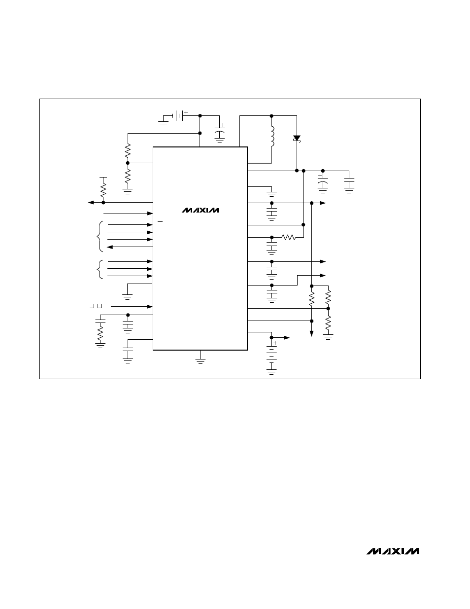
MAX769
2 OR 3-CELL
AA ALKALINE
BATTERY
BATT
26
1
11
6
9
27
5
2
3
28
25
4
24
22
14
21
20
10
7
23
15
C
OFS
0.1
µ
F
3.0V
LOGIC
2.85V
ANALOG
1V RCVR
R4
470k
R3
1.3M
100k
3-CELL
NiCd
TO RF
PA
R
OFS
, 15k
LX2
OUT
PGND
REG1
R2IN
OFS
REG2
L1
68
µ
H
D1
MBR0520L
C6
0.1
µ
F
C1
47
µ
F
C2
10
µ
F
C3
10
µ
F
TO
µ
C
RESET
C4
1
µ
F
C5
22
µ
F
SERIAL
I/O
A/D IN
R5
270k
17
19
18
16
13
12
8
1.8
Ω
DRIVERS
38.4kHz
C10
22nF
C8
1
µ
F
C9
1nF
REG3
RSIN
RSO
NICD
AGND
LBI
R1
1M
R2
250k
REG1
LBO
CH0
CS
SCL
SDI
SDO
DR1
DR2
DR2IN
DRGND
SYNC
FILT
REF
LX1
10k
Figure 2. Standard Application Circuit