Table 5. v, Output voltage, Automatic backup – Rainbow Electronics MAX769 User Manual
Page 13: Serial interface
MAX769
2 or 3-Cell, Step-Up/Down,
Two-Way Pager System IC
______________________________________________________________________________________
13
All DC-DC converter and charging circuitry is disabled
when the backup regulator is turned on, but all other
functions remain active. Activate BACKUP manually or by
serial command, or set it to trigger automatically via LBO.
Automatic Backup
Setting the LBO_Sets_BACKUP serial bit (Table 1) pro-
grams the IC so that when LBO goes low, the backup
regulator automatically turns on without instructions from
the microprocessor (µP). When the LBO_Sets_BACKUP
bit is 0, the backup regulator is turned on only by setting
the BACKUP bit. The BACKUP bit also overrides the
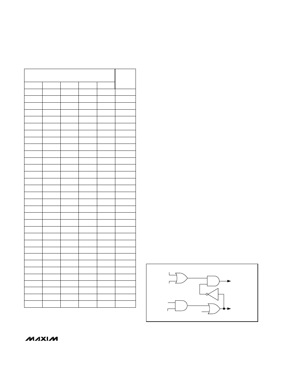
LBO_Sets_BACKUP bit. Figure 3 shows the logic for this
function.
If the main battery is depleted and the NiCd battery is
drained during backup, RSO goes low while the back-
up regulator is supplying OUT (if RSI is used to monitor
OUT or REG1). When RSO falls, the serial registers
reset to their POR states (with the DC-DC converter on
in Coast Mode and the backup regulator off, see
Tables 1, 2, and 3). This prevents the IC from getting
hung up with the DC-DC converter off when a new main
battery is inserted. This sequence is required because
if the MAX769 did not default to “DC-DC converter on”
when coming out of reset, the µP (still reset by RSO)
would not be able to provide the device with serial
instructions to turn on.
Serial Interface
The MAX769 has an SPI-compatible serial interface.
The serial-interface lines are Chip Select (CS), Serial
Clock (SCL), Serial Data In (SDI), and Serial Data Out
(SDO). Serial input data is arranged in 8-bit bytes. Most
bytes contain a 3-bit address pointer (R2, R1, R0)
along with 5 bits of input data (D4–D0). For common
operations such as selecting Run or Coast Mode, acti-
vating REG2 or REG3, or turning on DR1 or DR2, only
the 000 (R2, R1, R0) address register needs to be writ-
ten. The serial input data format for all MAX769 opera-
tions is outlined in Tables 1, 2, and 3.
15mA_CHG
1mA_CHG
TO
CHARGER
CONTROL
TO
BACKUP
REGULATOR
BACKUP
LBO_SETS_BACKUP
LBO
Figure 3. Logic for Charger Control and BACKUP and for
LBO_Sets_BACKUP Serial Input Bits
2.5
1
0
1
1
0
4.9
1
1
1
1
1
4.8
1
1
0
1
1
4.7
0
1
1
1
1
4.6
0
1
0
1
1
4.5
1
1
1
0
1
4.4
1
1
0
0
1
4.3
0
1
1
0
1
4.2
0
1
0
0
1
4.1
1
0
1
1
1
4.0
1
0
0
1
1
3.9
0
0
1
1
1
3.8
0
0
0
1
1
3.7
1
0
1
0
1
3.6
1
0
0
0
1
3.5
0
0
1
0
1
3.4
0
0
0
0
1
3.3
1
1
1
1
0
3.2
1
1
0
1
0
3.1
0
1
1
1
0
3.0
0
1
0
1
0
2.9
1
1
1
0
0
2.8
1
1
0
0
0
2.7
0
1
1
0
0
2.6
0
1
0
0
0
2.4
1
0
0
1.9
1.8
1
0
V
OUT
(V)
2.3
0
0
0
0
OV1
1
1
0
2.2
0
0
0
OV3
0
0
1
0
2.1
1
0
1
0
0
2.0
1
0
0
0
0
0
OV0
OV2
OV4
1
0
0
0
0
Table 5. V
OUT
Output Voltage
SERIAL-DATA BIT