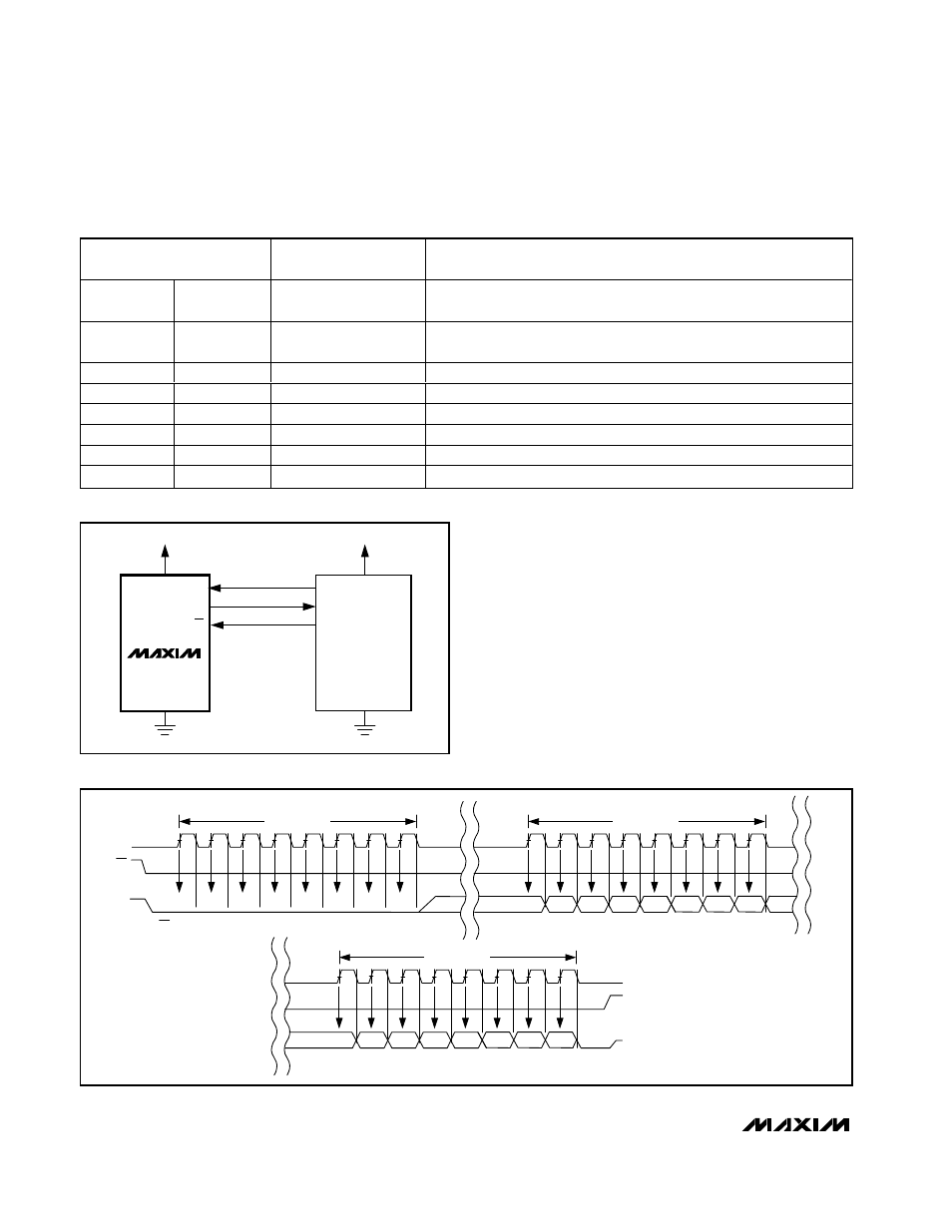
Table 8. detailed sspstat register contents, Dsp interface – Rainbow Electronics MAX1068 User Manual
Page 26

DSP Interface
The DSP mode of the MAX1068 only operates in exter-
nal clock mode. Figure 23 shows a typical DSP interface
connection to the MAX1068. Use the same oscillator as
the DSP to provide the clock signal for the MAX1068.
The DSP provides the falling edge at CS to wake the
MAX1068. The MAX1068 detects the state of DSPR on
the falling edge of CS (Figure 17). Logic low at DSPR
places the MAX1068 in DSP mode. After the MAX1068
enters DSP mode, CS can be left low. A frame sync
pulse from the DSP to DSPR initiates a conversion. The
MAX1068 sends a frame sync pulse from DSPX to the
DSP signaling that the MSB is available at DOUT. Send
another frame sync pulse from the DSP to DSPR to
begin the next conversion. The MAX1068 does not
operate in scan mode when using DSP mode.
MAX1067/MAX1068
Multichannel, 14-Bit, 200ksps Analog-to-Digital
Converters
26
______________________________________________________________________________________
DOUT*
CS
SCLK
1ST BYTE READ
2ND BYTE READ
*WHEN CS IS HIGH, DOUT = HIGH-Z
MSB
HIGH-Z
3RD BYTE READ
LSB
S1
S0
D5
D4
D3
D2
D1
D0
24
20
16
12
8
6
4
1
D13
D12
D11
D10
D9
D8
D7
D6
0
0
0
0
0
0
0
0
Figure 22b. SPI Interface Timing with PIC16/PIC17 in Master Mode (CKE = 1, CKP = 0, SMP = 0, SSPM3 - SSPM0 = 0001)
SCK
SDI
GND
PIC16/17
I/O
SCLK
DOUT
CS
V
DD
V
DD
MAX1067
MAX1068
Figure 22a. SPI Interface Connection for a PIC16/PIC17
CONTROL BIT
SETTINGS
SYNCHRONOUS SERIAL-PORT STATUS REGISTER (SSPSTAT)
SMP
BIT7
0
SPI Data-Input Sample Phase. Input data is sampled at the middle of
the data output time.
CKE
BIT6
1
SPI Clock Edge-Select Bit. Data is transmitted on the rising edge of the
serial clock.
D/A
BIT5
X
Data Address Bit
P
BIT4
X
Stop Bit
S
BIT3
X
Start Bit
R/W
BIT2
X
Read/Write Bit Information
UA
BIT1
X
Update Address
BF
BIT0
X
Buffer-Full Status Bit
Table 8. Detailed SSPSTAT Register Contents
X = Don’t care.
