Applications information – Rainbow Electronics MAX1068 User Manual
Page 23

MAX1067/MAX1068
Multichannel, 14-Bit, 200ksps Analog-to-Digital
Converters
______________________________________________________________________________________
23
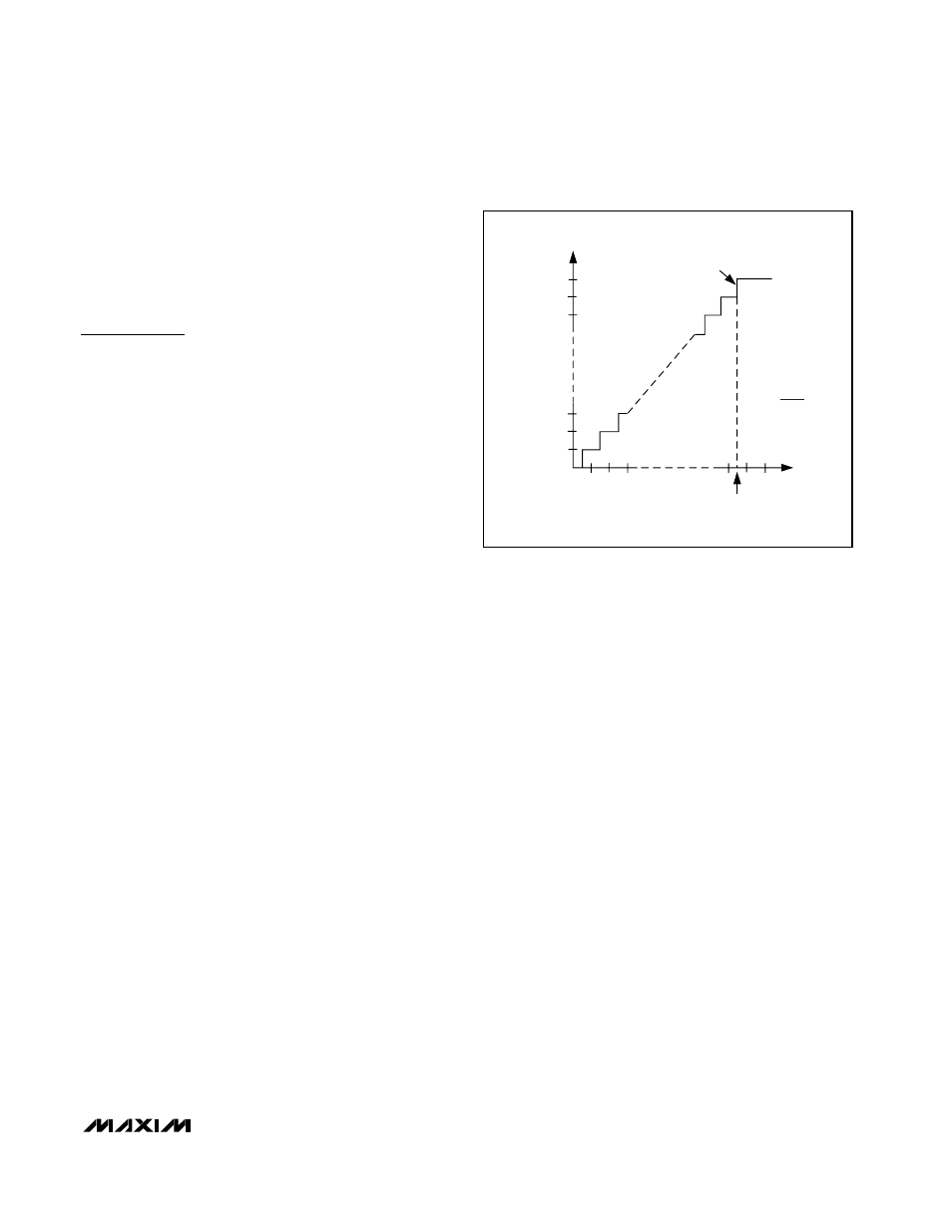
Output Coding and Transfer Function
The data output from the MAX1067/MAX1068 is
straight binary. Figure 19 shows the nominal transfer
function. Code transitions occur halfway between suc-
cessive integer LSB values (V
REF
= +4.096V, and
1 LSB = +250µV or 4.096V / 16,384V).
Applications Information
Internal Reference
The internal bandgap reference provides a buffered
+4.096V. Bypass REFCAP with a 0.1µF capacitor to
AGND and REF with a 1µF capacitor to AGND. For best
results, use low-ESR, X5R/X7R ceramic capacitors.
Allow 5ms for the reference and buffer to wake up from
full power-down (see Table 5).
External Reference
The MAX1067/MAX1068 accept an external reference
with a voltage range between +3.8V and AV
DD
.
Connect the external reference directly to REF. Bypass
REF to AGND with a 10µF capacitor. When not using a
low-ESR bypass capacitor, use a 0.1µF ceramic capac-
itor in parallel with the 10µF capacitor. Noise on the ref-
erence degrades conversion accuracy.
The input impedance at REF is 37k
Ω for DC currents.
During a conversion, the external reference at REF
must deliver 118µA of DC load current and have an
output impedance of 10
Ω or less.
For optimal performance, buffer the reference through
an op amp and bypass the REF input. Consider the
equivalent input noise (82µV
RMS
) of the MAX1067/
MAX1068 when choosing a reference.
Internal/External Oscillator
Select either an external (0.1MHz to 4.8MHz) or the
internal 4MHz (typ) clock to perform conversions
(Table 6). The external clock shifts data in and out of
the MAX1067/MAX1068 in either clock mode.
When using the internal clock mode, the internal oscil-
lator controls the acquisition and conversion process-
es, while the external oscillator shifts data in and out of
the MAX1067/MAX1068. Turn off the external clock
(SCLK) when the internal clock is on to realize lowest
noise performance. The internal clock remains off in
external clock mode.
Input Buffer
Most applications require an input-buffer amplifier to
achieve 14-bit accuracy. The input amplifier must have
a slew rate of at least 2V/µs and a unity-gain bandwidth
of at least 10MHz to complete the required output-volt-
age change before the end of the acquisition time.
At the beginning of the acquisition, the internal sam-
pling capacitor array connects to AIN_ (the amplifier
input), causing some disturbance on the output of the
buffer. Ensure the sampled voltage has settled before
the end of the acquisition time.
Digital Noise
Digital noise can couple to AIN_ and REF. The conver-
sion clock (SCLK) and other digital signals active during
input acquisition contribute noise to the conversion
result. Noise signals, synchronous with the sampling
interval, result in an effective input offset. Asynchronous
signals produce random noise on the input, whose high-
frequency components can be aliased into the frequen-
cy band of interest. Minimize noise by presenting a low
impedance (at the frequencies contained in the noise
signal) at the inputs. This requires bypassing AIN_ to
AGND, or buffering the input with an amplifier that has a
small-signal bandwidth of several megahertz (doing both
is preferable). AIN has a typical bandwidth of 4MHz.
OUTPUT CODE
FULL-SCALE
TRANSITION
11...111
1
2
3
0
FS
FS - 3/2 LSB
FS = V
REF
INPUT VOLTAGE (LSB)
1 LSB =
V
REF
16,384
11...110
11...101
00...011
00...010
00...001
00...000
Figure 19. Unipolar Transfer Function, Full Scale (FS) = V
REF
,
Zero Scale (ZS) = GND
