Rainbow Electronics MAX1068 User Manual
Page 19

sition. Use the EOC high-to-low transition as the signal
to restart the external clock (SCLK). To read the entire
conversion result, 16 SCLK cycles are needed. Extra
clock pulses, occurring after the conversion result has
been clocked out and prior to the rising edge of CS,
cause the conversion result to be shifted out again. The
MAX1067/MAX1068 internal clock 8-bit-wide data-
transfer mode requires 24 external clock cycles and 25
internal clock cycles for completion.
Force CS high after the conversion result is read. For
maximum throughput, force CS low again to initiate the
next conversion immediately after the specified mini-
mum time (t
CSW
). Forcing CS high in the middle of a
conversion immediately aborts the conversion and
places the MAX1067/MAX1068 in shutdown.
Scan mode allows multiple channels to be scanned
consecutively or one channel to be scanned eight
times. Scan mode can only be enabled when using the
MAX1067/MAX1068 in the internal clock mode. Enable
scanning by setting bits 4 and 3 in the command/con-
figuration/control register (see Tables 3 and 4). In scan
mode, conversion results are stored in memory until the
completion of the last conversion in the sequence.
Upon completion of the last conversion in the
sequence, EOC transitions from high to low to indicate
the end of the conversion and shuts down the internal
oscillator. Use the EOC high-to-low transition as the sig-
nal to restart the external clock (SCLK). DOUT provides
the conversion results in the same order as the channel
conversion process. The MSB of the first conversion is
available at DOUT on the falling edge of EOC (Figure 14).
MAX1067/MAX1068
Multichannel, 14-Bit, 200ksps Analog-to-Digital
Converters
______________________________________________________________________________________
19
DOUT
CS
SCLK
DIN
EOC
X X X X X X X X
DATA
LSB
S1 S0
X
t
ACQ
CONFIGURATION
X = DON
,
T CARE
DSPR = DSEL = DV
DD
t
CONV
POWER-DOWN
ADC
STATE
INTERNAL
CLK
1
8
9
16
2
13
32
24
17
32
• • •
• • •
• • •
• • •
MSB
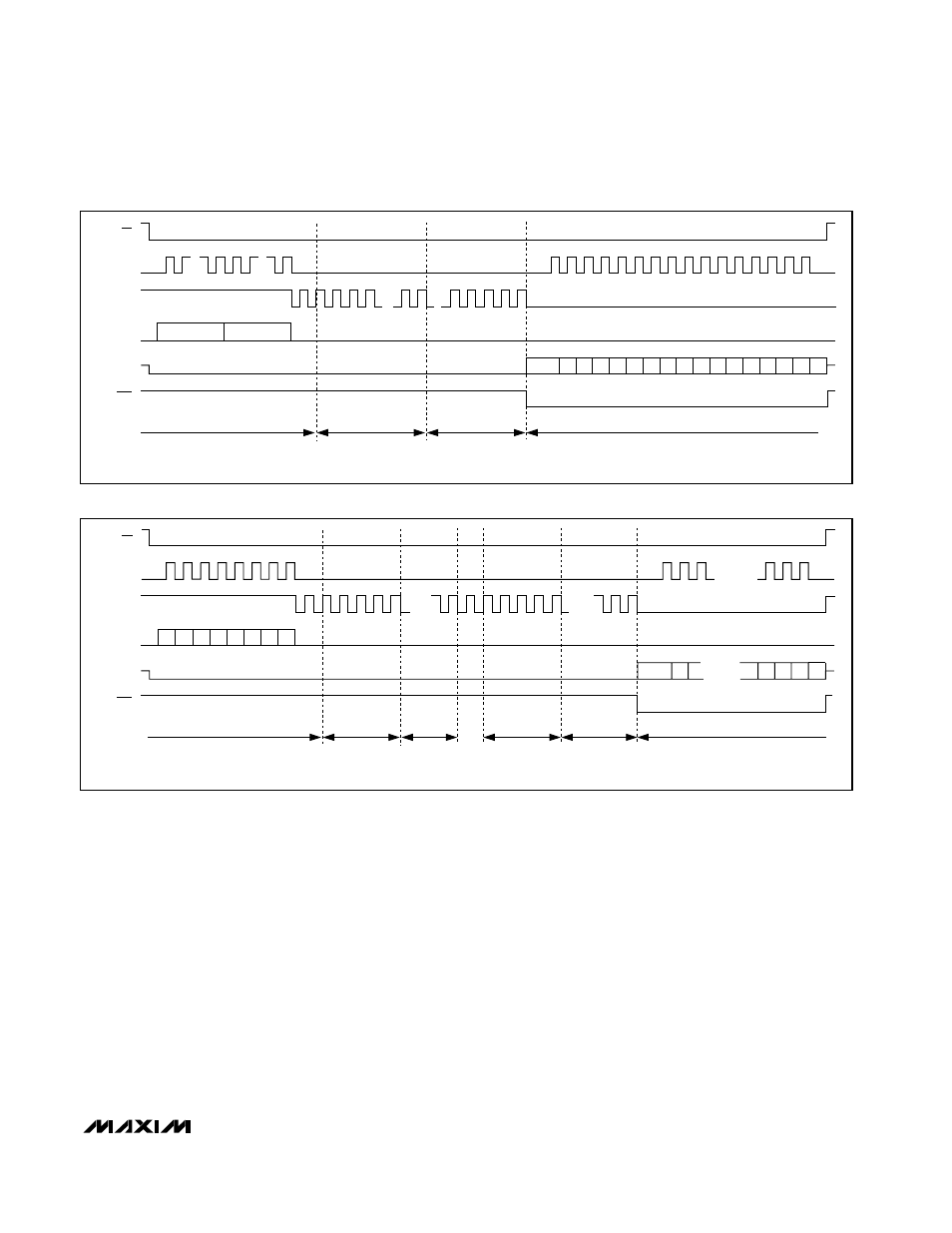
Figure 13. SPI Internal Clock Mode,16-Bit Data-Transfer Mode, Conversion Timing (MAX1068 Only)
DOUT
CS
SCLK
DIN
EOC
ADC
STATE
INTERNAL
CLK
1
8
9
40
• • •
• • •
2
6
24
48
30
26
• • •
• • •
1
MSB
LSB
LSB
S1 S0
X
MSB
t
ACQ
CONFIGURATION
POWER-DOWN
t
CONV
t
ACQ
t
CONV
X = DON
,
T CARE
DSPR = DV
DD
, DSEL = GND (MAX1068 ONLY)
Figure 14. SPI Internal Clock Mode, 8-Bit Data-Transfer Mode, Scan Mode for Two Conversions, Conversion Timing
