Serial interfaces – Rainbow Electronics MAX1068 User Manual
Page 24
MAX1067/MAX1068
Multichannel, 14-Bit, 200ksps Analog-to-Digital
Converters
24
______________________________________________________________________________________
Distortion
Avoid degrading dynamic performance by choosing an
amplifier with distortion much less than the total harmonic
distortion of the MAX1067/MAX1068 at the frequencies of
interest (THD = -98db at 1kHz). If the chosen amplifier
has insufficient common-mode rejection, which results in
degraded THD performance, use the inverting configura-
tion (positive input grounded) to eliminate errors from this
source. Low-temperature-coefficient, gain-setting resis-
tors reduce linearity errors caused by resistance
changes due to self-heating. To reduce linearity errors
due to finite amplifier gain, use amplifier circuits with suf-
ficient loop gain at the frequencies of interest..
DC Accuracy
To improve DC accuracy, choose a buffer with an offset
much less than the MAX1067/MAX1068s’ offset (±10mV
max for +5V supply), or whose offset can be trimmed
while maintaining stability over the required tempera-
ture range.
Serial Interfaces
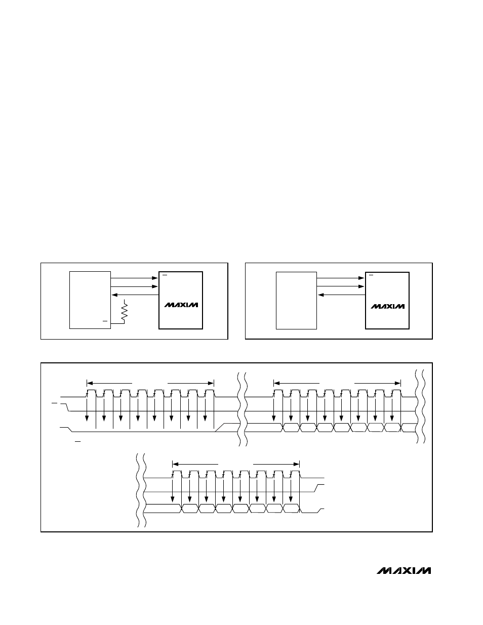
SPI and MICROWIRE Interfaces
When using the SPI (Figure 20a) or MICROWIRE (Figure
20b) interfaces, set CPOL = 0 and CPHA = 0. Drive CS
low to power on the MAX1067/MAX1068 before starting a
conversion (Figure 20c). Three consecutive 8-bit-wide
readings are necessary to obtain the entire 14-bit result
from the ADC. DOUT data transitions on the serial clock’s
falling edge. The first 8-bit-wide data stream contains all
leading zeros. The 2nd 8-bit-wide data stream contains
the MSB through D6. The 3rd 8-bit-wide data stream con-
tains D5 through D0 followed by S1 and S0.
CS
SCLK
DOUT
I/O
SCK
MISO
SPI
V
DD
SS
MAX1067
MAX1068
Figure 20a. SPI Connections
MAX1067
MAX1068
CS
MICROWIRE
SCLK
DOUT
I/O
SK
SI
Figure 20b. MICROWIRE Connections
DOUT*
CS
SCLK
1ST BYTE READ
2ND BYTE READ
*WHEN CS IS HIGH, DOUT = HIGH-Z
MSB
HIGH-Z
3RD BYTE READ
LSB
S1
S0
D5
D4
D3
D2
D1
D0
24
20
16
12
8
6
4
1
D13
D12
D11
D10
D9
D8
D7
D6
D5
0
0
0
0
0
0
0
0
Figure 20c. SPI/MICROWIRE Interface Timing Sequence (CPOL = CPHA = 0)