Voltage detectors bd48xxg/fve bd49xxg/fve – Rainbow Electronics BD4923G_FVE User Manual
Page 9
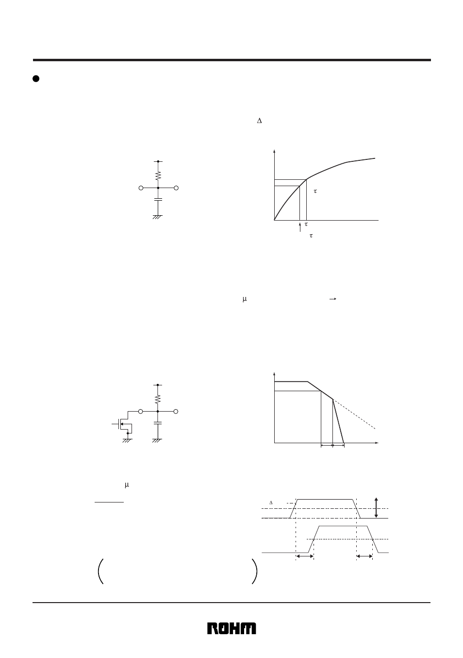
Establishment of RESET transfer delay time
• Delay time at the rise of V
DD
T
PLH
: Time until when V
OUT
is 1/2 of V
DD
after the rise of V
DD
, and beyond
the release voltage (Vs+ Vs).(See P7). It is the total time established
by IC internal transfer delay time T
D
and external R
L
, and C
L
.
• Delay time at the fall of V
DD
T
PHL
: Time until when V
OUT
is 1/2 of V
DD
after across the detection
voltage (Vs).(See P7). It is the total time established by IC internal
transfer delay time T
D
and external R
L
, and C
L
.
Delay time at the rise and fall of V
DD
can be established by R
L
, C
L
connected to V
OUT
pin.
If the threshold voltage of the RESET terminals is 1/2 of V
CC
, delay time T
PLH
at the rise of V
DD
is shown
in the expression below.
V
DD
RESET
Output Tr
OFF
OUT
C
L
R
L
T
PLH
=0.69 X C
L
X R
L
+T
D
T
D
=Internal circuit delay of BD48XX : About 35 s (typ.) V
DD
=(Vs–0.5V) (Vs+0.5V)
C
L
: Capacity of external capacitor beween V
OUT
pin and GND
R
L
: External resistance between V
OUT
pin and power supply
T
PHL
=A+B
A = About 70 s(Typ.) : Internal IC transfer delay time of BD4842
B =
CL X Vs
Delay time by external C
L
, R
L
IOL
C
L :
Capacity of external capacitor beween
VOUT pin and GND
Vs : Detection voltage
I
OL
: "L" output current of BD48XX
V
DD
RESET
Output Tr
ON
V
OUT
C
L
I
OL
R
L
Fig.24 RESET pin voltage
Fig.23
Fig.25
Fig.26 RESET pin voltage
Time
V
out v
oltage[V]
0
t
B
V
DD
Vs
A
RESET pin voltage
0
t
=C
L X
R
L
V
DD
Time
50%
0.69 X
63%
V
OUT
v
oltage [V]
Fig.27 Delay time I/O condition
Reference:V
S
=2.4V, V
DD
=About 8mA at A:typ.
Make sure to test in actual because it depends
on detection voltage.
:
9/15
Voltage detectors
BD48XXG/FVE
BD49XXG/FVE
Rev.A
Detection voltage V
S
[V]
0.5V
T
PLH
0.5V
5V
V
DD
Release voltage
(V
S
+ V
S
)
V
OUT
V
OUT
=5V X 0.5 [V]
T
PHL