Voltage detectors bd48xxg/fve bd49xxg/fve, Operating explanation when v, Is gradually decreased, output (v – Rainbow Electronics BD4923G_FVE User Manual
Page 5: Is gradually increased, output (v, Pin reaches each threshold voltage, v, Or other power supply. (in this case, output (v, H voltage is v, And output voltage v, When v, Sweep up for v
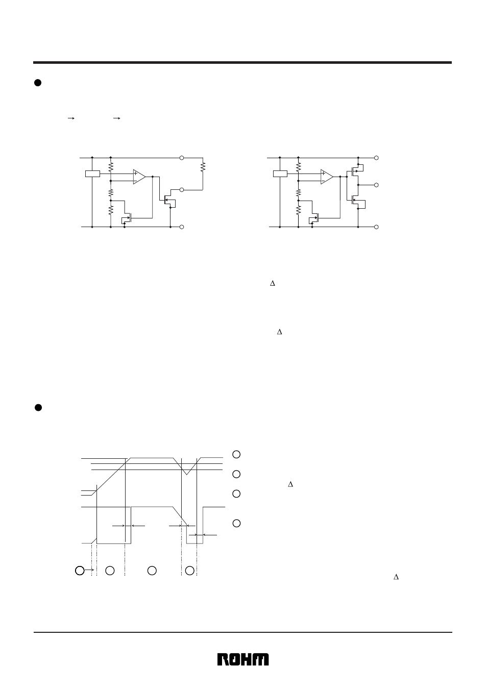
Operating explanation
When V
DD
is equal to or more than the release voltage (Vs+ Vs), output V
OUT
is in "H" mode. (Nch output
transistor Q1 is OFF, Pch output transistor Q2 is ON.) When V
DD
is gradually decreased, output (V
OUT
)
turns "L" in the detection voltage (Vs). (Nch output transistor Q1 is ON, Pch output transistor Q2 is OFF.)
When V
DD
is equal to or lower than the detection voltage (Vs+ Vs), output V
OUT
is in "L" mode. (Nch output
transistor Q1 is ON, Pch output transistor Q2 is OFF.) When V
DD
is gradually increased, output (V
OUT
) turns
"H" in the release voltage (Vs). (Nch output transistor Q1 is OFF, Pch output transistor Q2 is ON.)
Ex.) For both open drain type (Fig.7) and CMOS output type (Fig.8), detection voltage and release voltage are
threshold voltage. When voltage applied to V
DD
pin reaches each threshold voltage, V
OUT
pin voltage goes
"H" "L" or "L" "H". BD48XXG/FVE series are open drain types and pull-up resistor must be connected
to V
DD
, or other power supply. (In this case, output (V
OUT
) H voltage is V
DD
, or other power supply voltage.)
Ex.) The relation between input voltage V
DD
and output voltage V
OUT
when V
DD
is increased and decreased
is shown below. (Circuit is shown above. Fig7, 8)
• SWEEP DOWN for V
DD
• SWEEP UP for V
DD
• Some hysteresis is given such a way that the release voltage is the detection voltage X (1.05 Typ.).
• The output becomes inconsistent if the V
DD
is equal to or lower than the operating limit voltage.
GND
R1
R2
R3
Q1
V
DD
V
OUT
R
L
V
ref
R1
R2
R3
Q1
Q2
V
DD
GND
V
OUT
Vref
Fig.7 (BD48XX type Internal block diagram)
Fig.8 (BD49XX Internal block diagram)
Timing waveform
If the V
DD
is equal to or lower than the operating limit
voltage (V
OPL
) at power-up, the output is inconsistent.
When the V
DD
is equal to or lower than the reset release
voltage (Vs+ Vs), V
OUT
=L.
When V
DD
exceeds the Reset Release Voltage, V
OUT
turns H with a delay of T
PLH
. See Fig. 15 and 17 for the
reference waveform.
If the V
DD
goes below the detection (Vs) at power-down
or instantaneous power failure, V
OUT
turns L with a delay
of T
PHL
.
Fig.9
V
DD
V
DD
V
OUT
V
S
0V
V
OPL
V
OH
T
PLH
V
OL
V
S
+ V
S
T
PHL
T
PLH
2
3
4
1
1
1
2
1
3
4
See Fig.16 and 18 for the reference waveform.
The potential difference between the detection voltage
and the release voltage is called hysteresis ( Vs).
The products are designed so as to prevent power supply
fluctuation within this hysteresis from causing fluctuation
in output in order to avoid malfunction due to noise.
5/15
Voltage detectors
BD48XXG/FVE
BD49XXG/FVE
Rev.A
D