Voltage detectors bd48xxg/fve bd49xxg/fve, And power supply for the reset detection (v, Is different. provide r – Rainbow Electronics BD4923G_FVE User Manual
Page 6: Side, it can be used, When the capacitor c, Rev.a
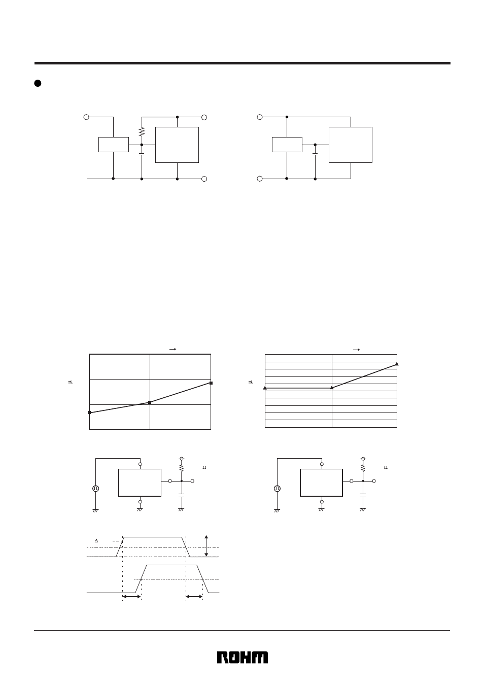
Application circuit
1)Application circuit as ordinal supply detection reset is shown below.
Output type of BD48XXG/FVE series (Open drain type) and BD49XXG/FVE series (CMOS type) is different.
An example of usage is shown below.
• When the power supply of microcontroller (V
DD2
) and power supply for the reset detection (V
DD1
) is different.
Provide R
L
for the output of a product with open drain output (BD48XXG/FVE series) on the V
DD2
side,
as shown in Fig.10.
• When the power supply of microcontroller and that of reset is same (V
DD1
).
A product with CMOS output (BD49XXG/FVE series) can be used as shown in Fig.11. Or if R
L
is provided
with open drain output (BD48XXG/FVE series) on the V
DD1
side, it can be used.
Fig.10 Open collector output type
Fig.11 CMOS output type
( )
BD48XXX
Micro
controller
V
DD2
V
DD1
R
L
R
ST
C
L
GND
( )
BD49XXX
V
DD1
C
L
GND
R
ST
10
100
1000
1000
100
10000
10000
Output delay time "L H"
C
L
Capacitance (pF)
dela
y time
( s)
[BD4842G/FVE]
10000
70
71
72
73
74
75
76
77
78
79
80
1000
100
C
L
Capacitance (pF)
Output delay time "H L"
dela
y time
( s)
[BD4842G/FVE]
Fig.14 Delay time I/O condition
5V
V
S
±0.5V
R
L
=100K
C
L
V
DD
V
OUT
GND
Fig.12
5V
V
S
±0.5V
R
L
=100K
C
L
V
DD
V
OUT
GND
Fig.13
Detection voltage V
S
[V]
0.5V
T
PLH
0.5V
5V
V
DD
Release voltage
(V
S
+ V
S
)
V
OUT
V
OUT
=5V X 0.5 [V]
T
PHL
(Noise filtering
capacitor)
(Noise filtering
capacitor)
Micro
controller
When the capacitor C
L
for noise filtering and for delay time setting is connected to V
OUT
pin (reset signal input
pin of microcontroller), make a setting in consideration of the wave rounding of the rise and fall of V
OUT
.
(See the delay shown in Fig.14 as the reference.)
6/15
Voltage detectors
BD48XXG/FVE
BD49XXG/FVE
Rev.A