Address registers and transfer status – Rainbow Electronics DS2433 User Manual
Page 3
DS2433
3 of 21
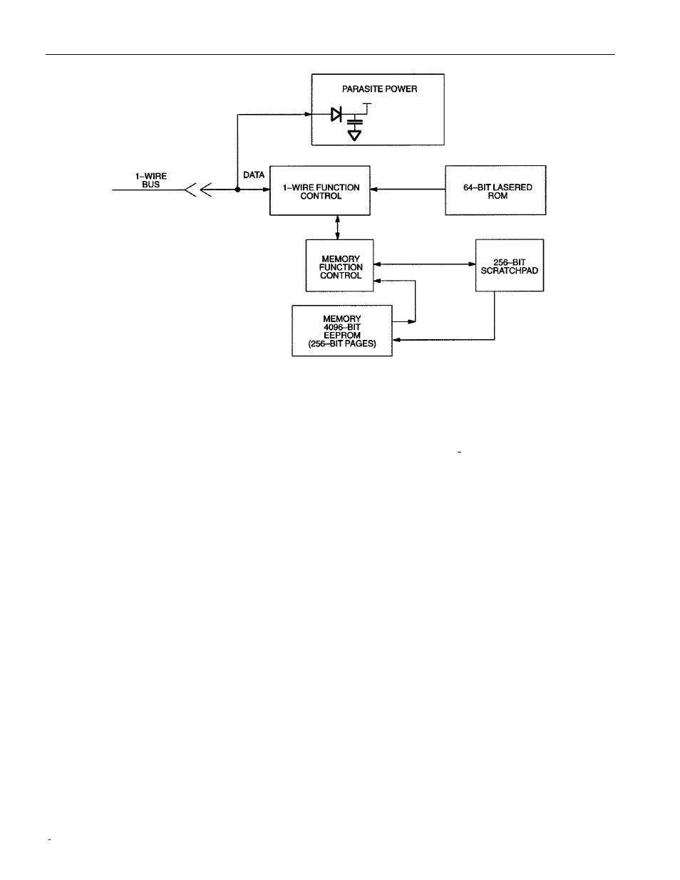
Figure 1. DS2433 BLOCK DIAGRAM
64-BIT LASERED ROM
Each DS2433 contains a unique ROM code that is 64 bits long. The first eight bits are a 1-Wire family
code. The next 48 bits are a unique serial number. The last eight bits are a CRC of the first 56 bits. (See
Figure 3.) The 1-Wire CRC is generated using a polynomial generator consisting of a shift register and
XOR gates as shown in Figure 4. The polynomial is X
8
+ X
5
+ X
4
+ 1. Additional information about the
Dallas 1-Wire Cyclic Redundancy Check is available in the Book of DS19xx iButton
®
Standards.
The shift register bits are initialized to zero. Then starting with the least significant bit of the family code,
one bit at a time is shifted in. After the 8
th
bit of the family code has been entered, then the serial number
is entered. After the 48
th
bit of the serial number has been entered, the shift register contains the CRC
value. Shifting in the eight bits of CRC should return the shift register to all zeros.
MEMORY
The memory map in Figure 5 shows a 32-byte page called the scratchpad and additional 32-byte pages
called memory. The DS2433 contains pages 0 through 15 that make up the 4096-bit EEPROM. The
scratch-pad is an additional page that acts as a buffer when writing to memory.
ADDRESS REGISTERS AND TRANSFER STATUS
Because of the serial data transfer, the DS2433 employs three address registers, called TA1, TA2 and E/S
(Figure 6). Registers TA1 and TA2 must be loaded with the target address to which the data will be
written or from which data will be sent to the master upon a Read command. Register E/S acts like a byte
counter and Transfer Status register. It is used to verify data integrity with write commands. Therefore,
the master only has read access to this register. The lower five bits of the E/S register indicate the address
of the last byte that has been written to the scratchpad. This address is called Ending Offset. Bit 5 of the
E/S register, called PF, is set if the number of data bits sent by the master is not an integer multiple of 8 or
if the data in the scratchpad is not valid due to a loss of power. A valid write to the scratchpad will clear
the PF bit. Bit 6 has no function; it always reads 0. Note that the lowest five bits of the target address also
determine the address within the scratchpad, where intermediate storage of data will begin. This address
is called byte offset. If the target address (TA1) for a Write command is 03CH for example, then the
scratchpad will store incoming data beginning at the byte offset 1CH and will be full after only four
iButton is a registered trademark of Dallas Semiconductor.