Ds1372, C, 32-bit, binary counter clock with 64-bit id, Pin description – Rainbow Electronics DS1372 User Manual
Page 4
DS1372
4
_______________________________________________________________________________________
Pin Description
PIN
NAME
FUNCTION
1, 2
X1, X2
Connections for Standard 32.768kHz Quartz Crystal. The internal oscillator circuitry is designed for
operation with a crystal having a 12.5pF specified load capacitance (C
L
). Pin X1 is the input to the
oscillator and can optionally be connected to an external 32.768kHz oscillator. The output of the
internal oscillator, pin X2, is floated if an external oscillator is connected to pin X1.
3 AD0
Slave Address Input. This pin is the slave address input for the I
2
C serial interface and is used to
access multiple devices on the same bus. To select the device, the address value on the pin
must match the corresponding bit in the device addresses. This pin can be connected to V
CC
or
ground or be driven to a logic-high or logic-low level.
4 GND
Ground
5 SDA
Serial Data Input/Output. This pin is the data input/output for the I
2
C serial interface. The SDA pin is
open drain and requires an external pullup resistor.
6 SCL
Serial Clock Input. This pin is the clock input for the I
2
C serial interface and is used to synchronize
data movement on the serial interface.
7 SQW/
INT
Square Wave or Active-Low Interrupt Open-Drain Output. This pin is used to output the square wave
or alarm interrupt signal. The function of this pin is selected by the state of the INTCN control bit.
This pin is open drain and requires an external pullup resistor.
8 V
CC
DC Power Pin. This pin should be decoupled using a 0.1μF or 1.0μF capacitor.
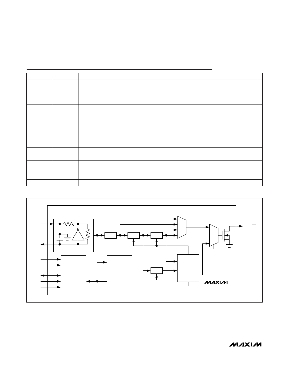
DS1372
OSCILLATOR
POWER
ч4096
ч4096
1Hz
1Hz
CLR
4096Hz
8192Hz
32,768Hz
DIVIDER CHAIN
RS[2:1]
X1
SQW/INT
V
CC
GND
SDA
SCL
AD0
X2
I
2
C
INTERFACE
CONTROL/
STATUS
32-BIT
COUNTER
24-BIT ALARM
COUNTER
64-BIT ID
ROM
ч2
ч4
MUX
INTCN
SQW
ACE
AF
MUX
N
Figure 1. Block Diagram
I
2
C, 32-Bit, Binary Counter Clock with 64-Bit ID