Ds1372, C, 32-bit, binary counter clock with 64-bit id, Electrical characteristics (continued) – Rainbow Electronics DS1372 User Manual
Page 3: Crystal specifications
DS1372
_______________________________________________________________________________________
3
Note 1:
Limits at -40°C are guaranteed by design and not production tested.
Note 2:
All voltages are referenced to ground.
Note 3:
SCL clocking at maximum frequency = 400kHz.
Note 4:
Specified with I
2
C bus inactive, SCL = SDA = V
CC
.
Note 5:
Measured with a 32.768kHz crystal attached to the X1 and X2 pins.
Note 6:
The I
2
C minimum operating frequency is imposed by the requirement of timeout period.
Note 7:
The first clock pulse is generated after this period.
Note 8:
A device must internally provide a hold time of at least 300ns for the SDA signal (referred to as the V
IHMIN
of the SCL sig-
nal) to bridge the undefined region of the falling edge of SCL.
Note 9:
The maximum t
HD:DAT
must only be met if the device does not stretch the low period (t
LOW
) of the SCL signal.
Note 10: A fast-mode device can be used in a standard-mode system, but the requirement t
SU:DAT
≥ 250ns must then be met.
This is automatically the case if the device does not stretch the low period of the SCL signal. If such a device does stretch
the low period of the SCL signal, it must output the next data bit to the SDA line t
R(MAX)
+ t
SU:DAT
= 1000 + 250 = 1250ns
before the SCL line is released.
Note 11: C
B
= Total capacitance of one bus line in pF.
Note 12: The parameter t
OSF
is the period of time the oscillator must be stopped for the OSF flag to be set over the voltage range of
2.4V
≤ V
CC
≤ V
CC(MAX)
.
Note 13: The DS1372 can detect any single SCL clock held low longer than T
_TIMEOUT
(MIN). The I
2
C interface is in reset state and
can receive a new START condition when SCL is held low for at least T
_TIMEOUT
(MAX). Once the part detects this condi-
tion the SDA output is released. The oscillator must be running for this function to work.
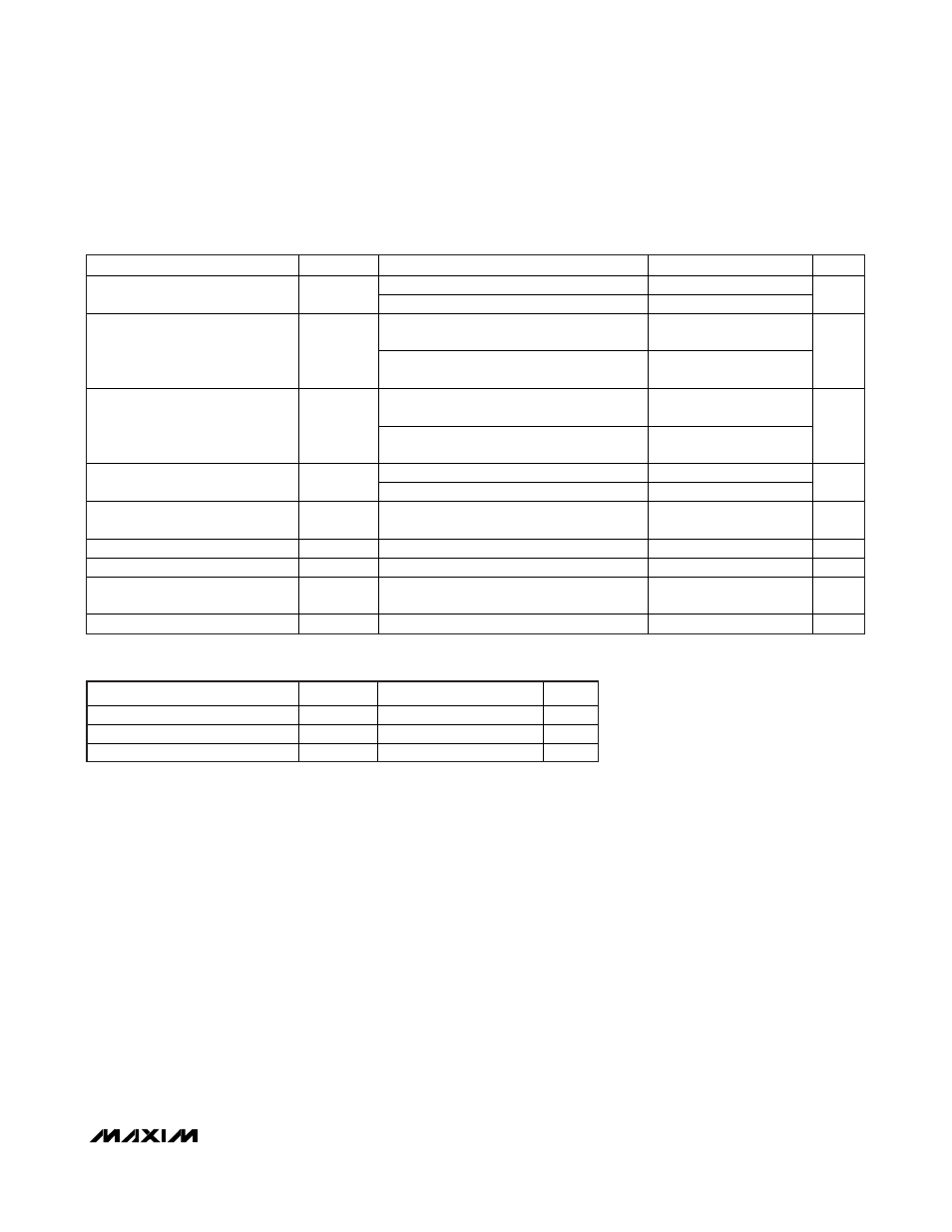
ELECTRICAL CHARACTERISTICS (continued)
(V
CC
= 2.4V to 5.5V, T
A
= -40°C to +85°C, unless otherwise noted.) (Note 1)
PARAMETER
SYMBOL
CONDITIONS
MIN
TYP
MAX
UNITS
Fast mode
100
Data Setup Time (Note 10)
t
SU:DAT
Standard mode
250
ns
Fast mode
20 +
0.1C
B
300
Rise Time of SDA and SCL
Signals (Note 11)
t
R
Standard mode
20 +
0.1C
B
1000
ns
Fast mode
20 +
0.1C
B
300
Fall Time of SDA and SCL Signals
(Note 11)
t
F
Standard mode
20 +
0.1C
B
300
ns
Fast mode
0.6
Setup Time for STOP Condition
t
SU:STO
Standard mode
4.0
μs
Capacitive Load for Each Bus
Line (Note 11)
C
B
400
pF
I/O Capacitance
C
I/O
10 pF
SCL
Spike
Suppresion
TSP
30 ns
Oscillator Stop Flag (OSF) Delay
(Note 12)
t
OSF
100 ms
Timeout Interval (Note 13)
T
_TIMEOUT
25 35
ms
CRYSTAL SPECIFICATIONS
PARAMETER
SYMBOL
MIN
TYP
MAX
UNITS
Nominal Frequency
f
O
32.768 kHz
Capacitive Load
C
L
12.5 pF
Equivalent
Series
Resistance ESR
50
k
I
2
C, 32-Bit, Binary Counter Clock with 64-Bit ID