Draft, Electrical characteristics (continued) – Rainbow Electronics ATA6626 User Manual
Page 20
20
4986B–AUTO–07/07
ATA6622/ATA6624/ATA6626 [Preliminary]
DRAFT
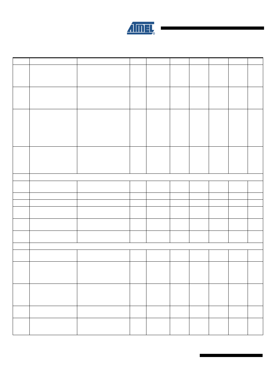
8.8
Input leakage current at
the receiver including
pull-up resistor as
specified
Input leakage current
Driver off
V
BUS
= 0V
V
Batt
= 12V
LIN
I
BUS_PAS_dom
–1
–0.35
mA
A
8.9
Leakage current LIN
recessive
Driver off
8V < V
Batt
< 18V
8V < V
BUS
< 18V
V
BUS
≥
V
Batt
LIN
I
BUS_PAS_rec
15
20
µA
A
8.10
Leakage current when
control unit disconnected
from ground.
Loss of local ground
must not affect
communication in the
residual network.
GND
Device
= V
S
V
Batt
= 12V
0V < V
BUS
< 18V
LIN
I
BUS_NO_gnd
–10
+0.5
+10
µA
A
8.11
Node has to sustain the
current that can flow
under this condition. Bus
must remain operational
under this condition.
V
Batt
disconnected
V
SUP_Device
= GND
0V < V
BUS
< 18V
LIN
I
BUS
5
15
µA
A
9
LIN Bus Receiver
9.1
Center of receiver
threshold
V
BUS_CNT
=
(V
th_dom
+ V
th
_
rec
)/2
LIN
V
BUS_CNT
0.475
×
V
S
0.5
×
V
S
0.525
×
V
S
V
A
9.2
Receiver dominant state V
EN
= 5V
LIN
V
BUSdom
0.4
×
V
S
V
A
9.3
Receiver recessive state V
EN
= 5V
LIN
V
BUSrec
0.6
×
V
S
V
A
9.4
Receiver input
hysteresis
V
hys
= V
th_rec
– V
th_dom
LIN
V
BUShys
0.028
×
V
S
0.1
×
V
S
0.175
×
V
S
V
A
9.5
Pre_Wake detection LIN
High-level input voltage
LIN
V
LINH
V
S
– 1V
V
S
+
0.3V
V
A
9.6
Pre_Wake detection LIN
Low-level input voltage
Activates the LIN receiver
LIN
V
LINL
–27
V
S
–
3.3V
V
A
10
Internal Timers
10.1
Dominant time for
wake-up via LIN bus
V
LIN
= 0V
t
bus
30
90
150
µs
A
10.2
Time delay for mode
change from Fail-safe
into Normal Mode via EN
pin
V
EN
= 5V
t
norm
5
15
20
µs
A
10.3
Time delay for mode
change from Normal
Mode to Sleep Mode via
EN pin
V
EN
= 0V
t
sleep
2
7
12
µs
A
10.4
TXD dominant time-out
timer (ATA6626 disabled)
V
TXD
= 0V
t
dom
6
13
20
ms
A
10.5
Time delay for mode
change from Silent Mode
into Normal Mode via EN
V
EN
= 5V
t
s_n
5
15
40
µs
A
8.
Electrical Characteristics (Continued)
5V < V
S
< 27V, -40°C < Tj < 150°C, unless otherwise specified. All values refer to GND pins
No.
Parameters
Test Conditions
Pin
Symbol
Min.
Typ.
Max.
Unit
Type*
*) Type means: A = 100% tested, B = 100% correlation tested, C = Characterized on samples, D = Design parameter