Absolute maximum ratings, Operating ratings (notes , ), Package thermal resistance – Rainbow Electronics ADC08L060 User Manual
Page 4: Converter electrical characteristics, Operating ratings
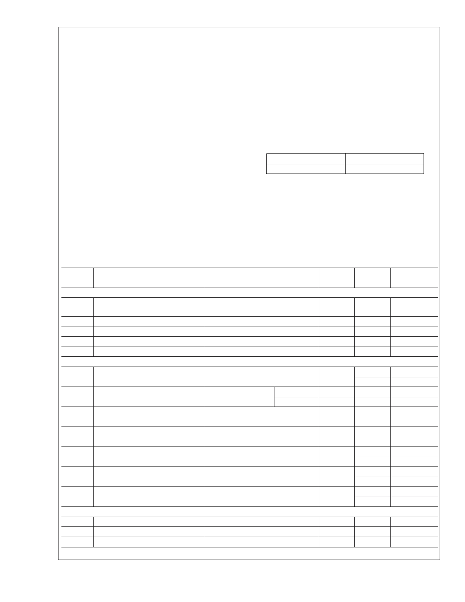
Absolute Maximum Ratings
(Notes 1, 2)
If Military/Aerospace specified devices are required,
please contact the National Semiconductor Sales Office/
Distributors for availability and specifications.
Supply Voltage (V
A
)
3.8V
Driver Supply Voltage (V
DR
)
V
A
+0.3V
Voltage on Any Input or Output Pin
−0.3V to V
A
Reference Voltage (V
RT
, V
RB
)
V
A
to AGND
CLK, PD Voltage Range
−0.05V to
(V
A
+ 0.05V)
Input Current at Any Pin (Note 3)
±
25 mA
Package Input Current (Note 3)
±
50 mA
Power Dissipation at T
A
= 25˚C
See (Note 4)
ESD Susceptibility (Note 5)
Human Body Model
Machine Model
2500V
200V
Soldering Temperature, Infrared,
10 seconds (Note 6)
235˚C
Storage Temperature
−65˚C to +150˚C
Operating Ratings
(Notes 1, 2)
Operating Temperature Range
−40˚C
≤ T
A
≤ +85˚C
Supply Voltage, V
A
+2.4V to +3.6V
Driver Supply Voltage, V
DR
+2.4V to V
A
Output Driver Voltage, V
DR
1.8V to V
A
Ground Difference |GND − DR GND|
0V to 300 mV
Upper Reference Voltage (V
RT
)
0.5V to (V
A
−0.3V)
Lower Reference Voltage (V
RB
)
0V to (V
RT
−0.5V)
V
IN
Voltage Range
V
RB
to V
RT
Package Thermal Resistance
Package
θ
JA
24-Lead TSSOP
92˚C/W
Converter Electrical Characteristics
The following specifications apply for V
A
= V
DR
= +3.0V
DC
, V
RT
= +1.9V, V
RB
= 0.3V, C
L
= 10 pF, f
CLK
= 60 MHz at 50% duty
cycle. Boldface limits apply for T
J
= T
MIN
to T
MAX
: all other limits T
J
= 25˚C (Notes 7, 8)
Symbol
Parameter
Conditions
Typical
Limits
Units
(Limits)
DC ACCURACY
INL
Integral Non-Linearity
+0.5
−0.2
+1.9
−1.35
LSB (max)
LSB (min)
DNL
Differential Non-Linearity
±
0.25
±
0.90
LSB (max)
Missing Codes
0
(max)
FSE
Full Scale Error
3.0
±
13
mV (max)
V
OFF
Zero Scale Offset Error
19
27
mV (max)
ANALOG INPUT AND REFERENCE CHARACTERISTICS
V
IN
Input Voltage
1.6
V
RB
V (min)
V
RT
V (max)
C
IN
V
IN
Input Capacitance
V
IN
= 0.75V +0.5
Vrms
(CLK LOW)
3
pF
(CLK HIGH)
4
pF
R
IN
R
IN
Input Resistance
>
1
M
Ω
BW
Full Power Bandwidth
270
MHz
V
RT
Top Reference Voltage
1.9
V
A
V (max)
0.5
V (min)
V
RB
Bottom Reference Voltage
0.3
V
RT
− 0.5
V (max)
0
V (min)
R
REF
Reference Ladder Resistance
V
RT
to V
RB
720
590
Ω (min)
1070
Ω (max)
I
ref
Reference Ladder Current
V
RT
to V
RB
2.2
1.5
mA (min)
2.7
mA (max)
CLK, PD DIGITAL INPUT CHARACTERISTICS
V
IH
Logical High Input Voltage
V
DR
= V
A
= 3.6V
2.0
V (min)
V
IL
Logical Low Input Voltage
V
DR
= V
A
= 2.7V
0.8
V (max)
I
IH
Logical High Input Current
V
IH
= V
DR
= V
A
= 3.6V
10
nA
ADC08L060
www.national.com
4