0 power supply considerations, 0 the digital input pins, 1 the pd pin – Rainbow Electronics ADC08L060 User Manual
Page 15: 2 the adc08l060 clock, 1 clock duty cycle, Applications information

Applications Information
(Continued)
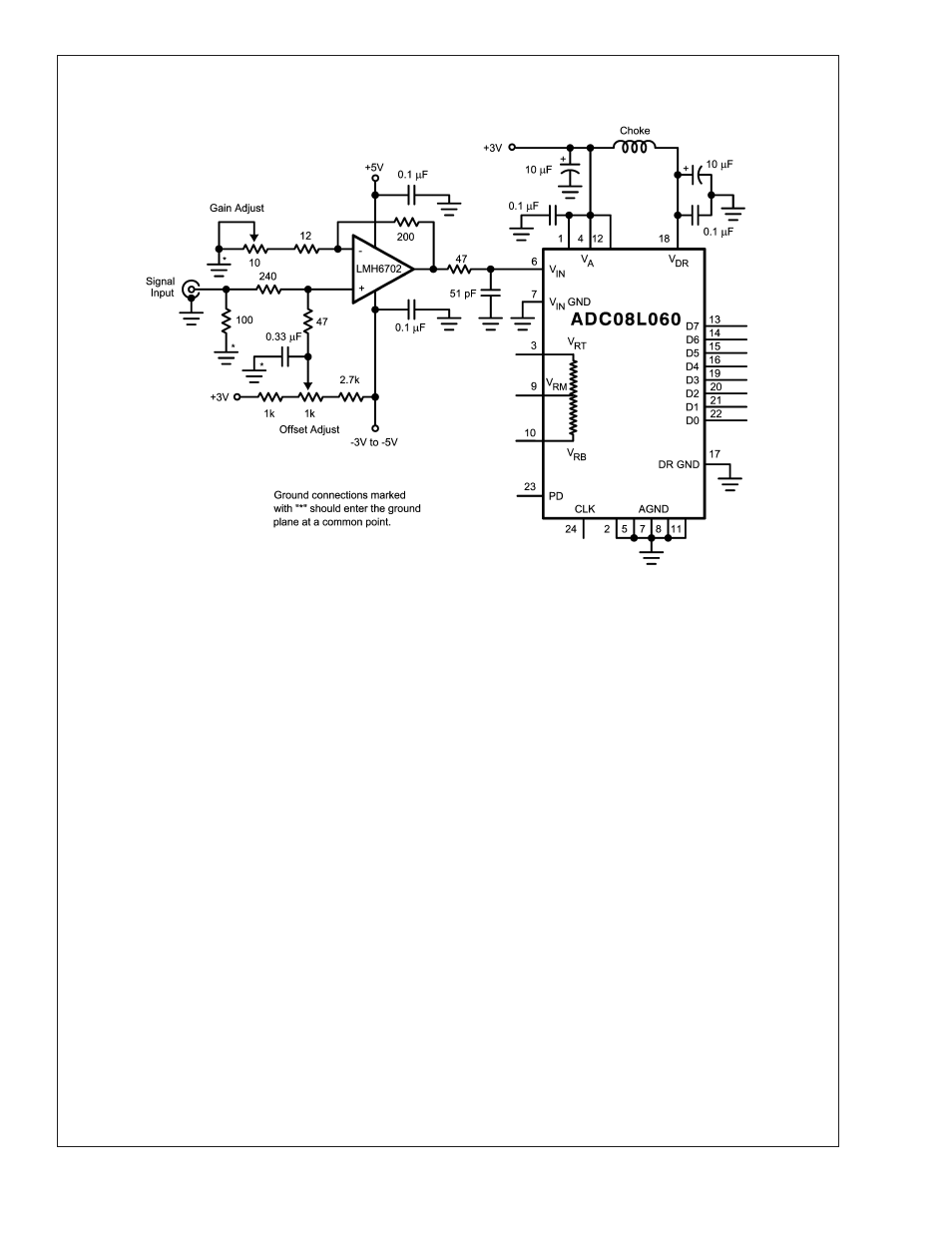
3.0 POWER SUPPLY CONSIDERATIONS
A/D converters draw sufficient transient current to corrupt
their own power supplies if not adequately bypassed. A
10 µF tantalum or aluminum electrolytic capacitor should be
placed within an inch (2.5 cm) of the A/D power pins, with a
0.1 µF ceramic chip capacitor placed within one centimeter
of the converter’s power supply pins. Leadless chip capaci-
tors are preferred because they have low lead inductance.
While a single voltage source is recommended for the V
A
and V
DR
supplies of the ADC08L060, these supply pins
should be well isolated from each other to prevent any digital
noise from being coupled into the analog portions of the
ADC. A choke or 27
Ω resistor is recommended between
these supply lines with adequate bypass capacitors close to
the supply pins.
As is the case with all high speed converters, the
ADC08L060 should be assumed to have little power supply
rejection. None of the supplies for the converter should be
the supply that is used for other digital circuitry in any system
with a lot of digital power being consumed. The ADC sup-
plies should be the same supply used for other analog
circuitry.
No pin should ever have a voltage on it that is in excess of
the supply voltage or below ground by more than 300 mV,
not even on a transient basis. This can be a problem upon
application of power and power shut-down. Be sure that the
supplies to circuits driving any of the input pins, analog or
digital, do not come up any faster than does the voltage at
the ADC08L060 power pins.
4.0 THE DIGITAL INPUT PINS
The ADC08L060 has two digital input pins: The PD pin and
the Clock pin.
4.1 The PD Pin
The Power Down (PD) pin, when high, puts the ADC08L060
into a low power mode where power consumption is reduced
to 1.4 mW with the clock running, or to about 1 mW with the
clock held low. Output data is valid and accurate about 1
microsecond after the PD pin is brought low.
The digital output pins retain the last conversion output code
when either the clock is stopped or the PD pin is high.
4.2 The ADC08L060 Clock
Although the ADC08L060 is tested and its performance is
guaranteed with a 60 MHz clock, it typically will function well
with clock frequencies from 10 MHz to 80 MHz.
4.2.1 Clock Duty Cycle
The low and high times of the clock signal can affect the
performance of any A/D Converter. Because achieving a
precise duty cycle is difficult, the ADC08L060 is designed to
maintain performance over a range of duty cycles. While it is
specified and performance is guaranteed with a 50% clock
duty cycle and 60 Msps, ADC08L060 performance is typi-
cally maintained with clock high and low times of 0.83 ns,
corresponding to a clock duty cycle range of 5% to 95% with
a 60 MHz clock. Note that minimum low and high times may
not be simultaneously asserted.
20041734
FIGURE 4. The input amplifier should incorporate some gain for best performance (see text).
ADC08L060
www.national.com
15
