0 the analog input, Applications information – Rainbow Electronics ADC08L060 User Manual
Page 14
Applications Information
(Continued)
2.0 THE ANALOG INPUT
The analog input of the ADC08L060 is a switch followed by
an integrator. The input capacitance changes with the clock
level, appearing as 3 pF when the clock is low, and 4 pF
when the clock is high. The sampling nature of the analog
input causes current spikes that result in voltage spikes at
the analog input pin. Any circuit used to drive the analog
input must be able to drive that input and to settle within the
clock low time. The LMH6702 has been found to be a good
amplifier to drive the ADC08L060.
Figure 4 shows an example of an input circuit using the
LMH6702. Any input amplifier should incorporate some gain
as operational amplifiers exhibit better phase margin and
transient response with gains above 2 or 3 than with unity
gain. If an overall gain of less than 3 is required, attenuate
the input and operate the amplifier at a higher gain, as
shown in Figure 4.
The RC at the amplifier output filters the clock rate energy
that comes out of the analog input due to the input sampling
circuit. The optimum time constant for this circuit depends
not only upon the amplifier and ADC, but also on the circuit
layout and board material. A resistor value should be chosen
between 10
Ω and 47Ω and the capacitor value chose ac-
cording to the formula
This will provide optimum SNR performance. Best THD per-
formance is realized when the capacitor and resistor values
are both zero. To optimize SINAD, reduce the capacitor
value until SINAD performance is optimized. That is, until
SNR = −THD. This value will usually be in the range of 20&
to 65% of the value calculated with the above formula. An
accurate calculation is not possible because of the board
material and layout dependence.
The circuit of Figure 4 has both gain and offset adjustments.
If you eliminate these adjustments normal circuit tolerances
may result in signal clipping unless care is exercised in the
worst case analysis of component tolerances and the input
signal excursion is appropriately limited to account for the
worst case conditions.
20041733
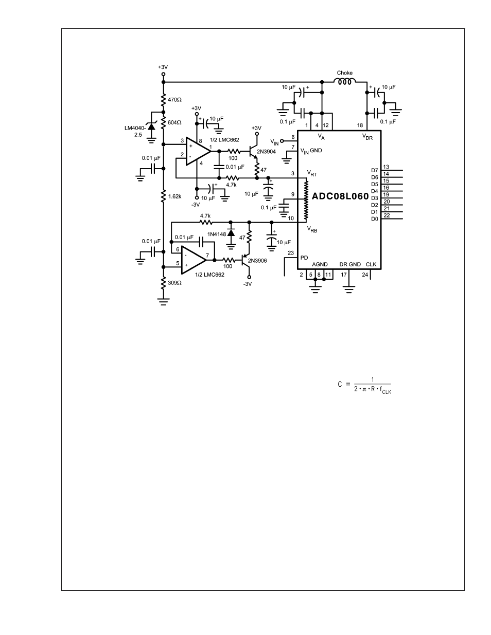
FIGURE 3. Driving the reference to force desired values requires driving with a low impedance source.
ADC08L060
www.national.com
14