Functional description, Applications information, 0 reference inputs – Rainbow Electronics ADC08L060 User Manual
Page 13
Functional Description
The ADC08L060 uses a unique architecture that achieves
over 7 effective bits at input frequencies up to and beyond
Nyquist.
The analog input signal that is within the voltage range set by
V
RT
and V
RB
is digitized to eight bits. Input voltages below
V
RB
will cause the output word to consist of all zeroes. Input
voltages above V
RT
will cause the output word to consist of
all ones.
Incorporating
a
switched
capacitor
bandgap,
the
ADC08L060 exhibits a power consumption that is propor-
tional to frequency, limiting power consumption to what is
needed at the clock rate that is used. This and its excellent
performance over a wide range of clock frequencies makes
it an ideal choice as a single ADC for many 8-bit needs.
Data is acquired at the rising edge of the clock and the digital
equivalent of that data is available at the digital outputs 5
clock cycles plus t
OD
later. The ADC08L060 will convert as
long as an adequate clock signal is present at pin 24. The
device is in the active state when the Power Down pin (PD)
is low. When the PD pin is high, the device is in the power
down mode, where the output pins hold the last conversion
before the PD pin went high and the device consumes about
1.4 mW. Holding the clock input low will further reduce the
power consumption in the power down mode to about 1 mW
Applications Information
1.0 REFERENCE INPUTS
The reference inputs V
RT
and V
RB
are the top and bottom of
the reference ladder, respectively. Input signals between
these two voltages will be digitized to 8 bits. External volt-
ages applied to the reference input pins should be within the
range specified in the Operating Ratings table. Any device
used to drive the reference pins should be able to source
sufficient current into the V
RT
pin and sink sufficient current
from the V
RB
pin to keep these voltages stable.
The reference bias circuit of Figure 2 is very simple and the
performance is adequate for many applications. However,
circuit tolerances will lead to a wide reference voltage range.
Better reference stability can be achieved by driving the
reference pins with low impedance sources.
The circuit of Figure 3 will allow a more accurate setting of
the reference voltages. The lower amplifier must have bipo-
lar supplies as its output voltage must go negative to force
V
RB
to any voltage below the V
BE
of the PNP transistor. Of
course, the divider resistors at the amplifier input could be
changed to suit your reference voltage needs, or the divider
can be replaced with potentiometers for precise settings.
The bottom of the ladder (V
RB
) may simply be returned to
ground if the minimum input signal excursion is 0V. Be sure
that the driving source can source sufficient current into the
V
RT
pin and sink enough current from the V
RB
pin to keep
these pins stable.
The LMC662 amplifier shown was chosen for its low offset
voltage and low cost. V
RT
should always be at least 0.5V
more positive than V
RB
to minimize noise.
The V
RM
pin is the center of the reference ladder and should
be bypassed to a quiet point in the analog ground plane with
a 0.1 µF capacitor. DO NOT allow this pin to float.
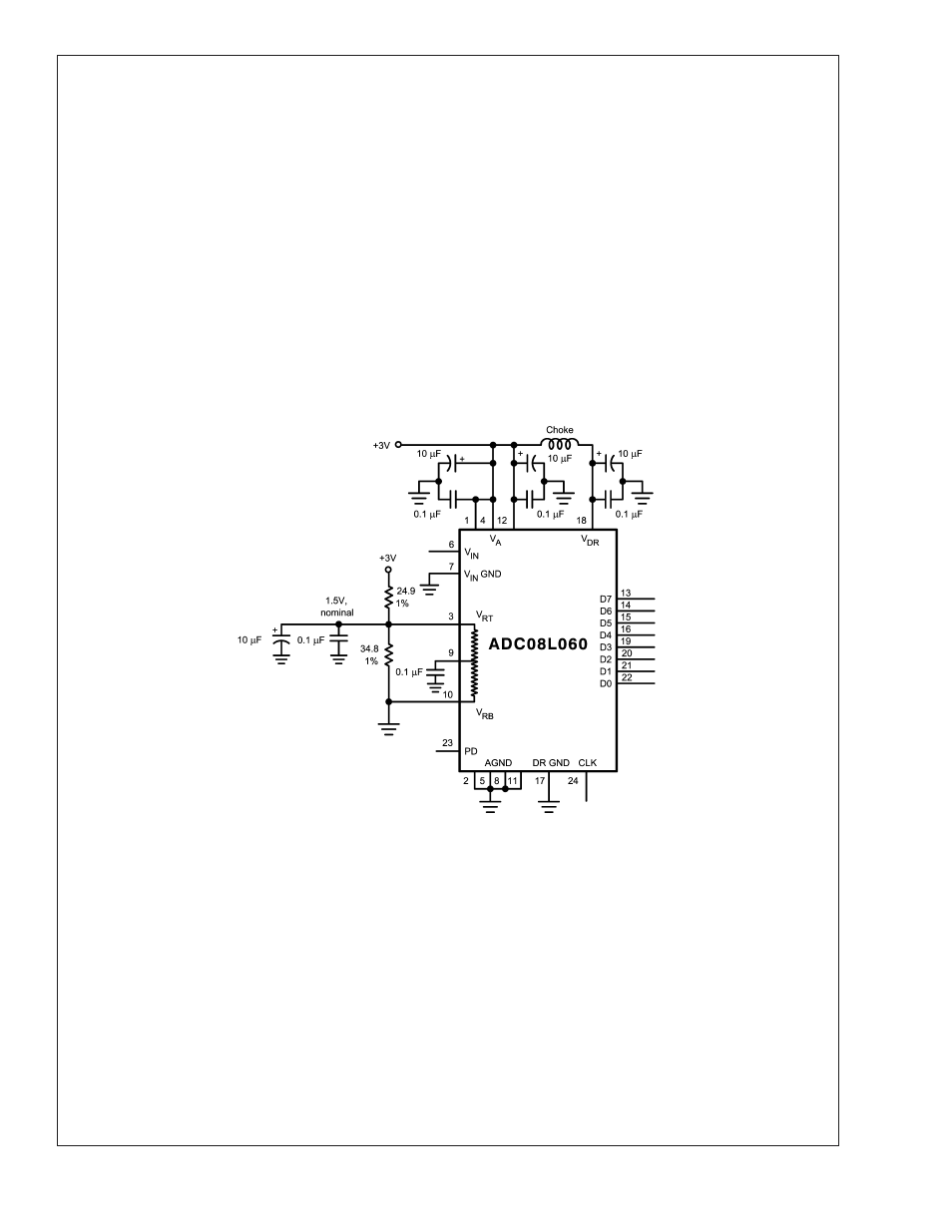
20041732
FIGURE 2. Simple, low component count reference biasing. Because of the ladder and external resistor tolerances,
the reference voltage of this circuit can vary too much for some applications.
ADC08L060
www.national.com
13