Rainbow Electronics ISD4004 User Manual
Page 25

ISD4004 Series
21
ISD
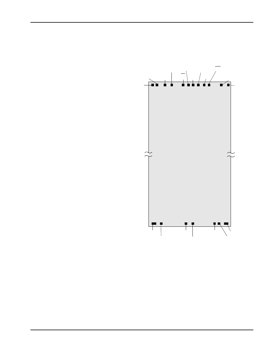
Figure 15: ISD4004 Series Bonding Physical Layout
1
(Unpackaged Die)
1. The backside of die is internally connected to V
SS
. It MUST NOT be connected to any other potential or damage
may occur.
2. Double bond recommended.
3. This figure reflects the current die thickness. Please contact ISD as this thickness may change in the future.
ISD4004 Series
I.
Die Dimensions
X: 4230 microns
Y: 9780 microns
II.
Die Thickness
(3)
11.5 ±0.5 mils
III. Pad Opening (min)
90 x 90 microns
3.5 x 3.5 mils
V
CCD1
V
SSA
AUD OUT
AM CAP
ANA IN–
INT
V
SSA
XCLK
V
CCD2
SS
MOSI
MISO
V
SSD2
V
SSD1
ISD4004
RAC
SCLK
V
SSA
(2)
ANA IN+
V
CCA
(2)
