Rainbow Electronics ISD4004 User Manual
Page 17

ISD4004 Series
13
ISD
1. Typical values: T
A
= 25°C and 3.0 V.
2. All min/max limits are guaranteed by ISD via electrical testing or characterization. Not all specifications are 100
percent tested.
3. Low-frequency cut off depends upon the value of external capacitors (see Pin Descriptions).
4. Single-ended input mode. In the differential input mode, V
IN
maximum for ANA IN+ and ANA IN– is 16 mV peak-
to-peak.
5. Sampling Frequency and Duration can vary as much as ±2.25 percent over the commercial temperature and
voltage ranges. For greater stability, an external clock can be utilized (see Pin Descriptions).
6. Filter specification applies to the antialiasing filter and to the smoothing filter.
7. The typical output voltage will be approximately 570 mV peak-to-peak with V
IN
at 32 mV peak-to-peak.
8. For optimal signal quality, this maximum limit is recommended.
9. When a record command is sent, T
RAC
= T
RAC
+ T
RACLO
on the first row addressed.
1. Typical values: T
A
= 25°C and 3.0 V. Timing measured at 50 percent of the V
CC
level.
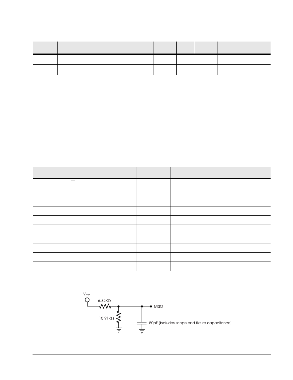
2. Tristate test condition.
THD
Total Harmonic Distortion
1
2
%
@ 1 KHz
V
IN
ANA IN Input Voltage
32
mV
Peak-to-Peak
(4) (7) (8)
Table 12: SPI AC Parameters
1
Symbol
Characteristics
Min
Max
Units
Conditions
T
SSS
SS Setup Time
500
nsec
T
SSH
SS Hold Time
500
nsec
T
DIS
Data in Setup Time
200
nsec
T
DIH
Data in Hold Time
200
nsec
T
PD
Output Delay
500
nsec
T
DF
(2)
Output Delay to hiZ
500
nsec
T
SSmin
SS HIGH
1
msec
T
SCKhi
SCLK High Time
400
nsec
T
SCKlow
SCLK Low Time
400
nsec
F
0
CLK Frequency
1,000
KHz
Table 11: AC Parameters (Die)
Symbol
Characteristic
Min
(2)
Typ
(1)
Max
(2)
Units
Conditions
