Voltage detectors bd52xxg/fve bd53xxg/fve, 1 detection voltage (v, Rev.a – Rainbow Electronics BD5323G_FVE User Manual
Page 4

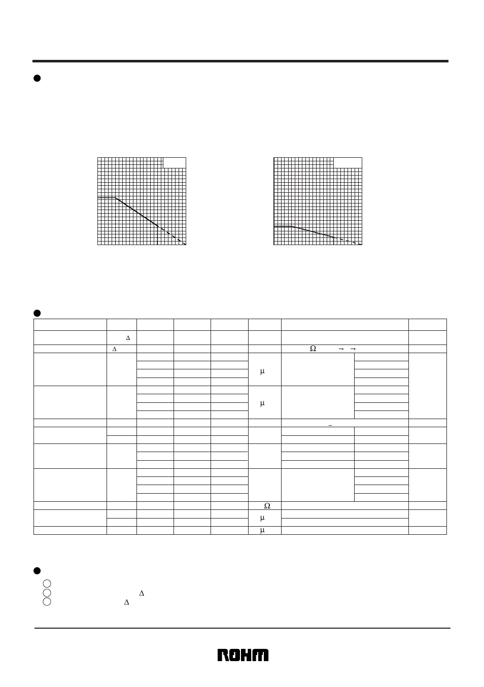
Power dissipation
When it is used in the ambient temperature of (Ta)=25°C and more, make reference to each thermal derating
characteristics of used package. Both Fig.5 and Fig.6 show these characteristic when ROHM's standard board
(70mmX70mmX1.6mm, glass epoxy board) is mounted.
Power consumption of the IC
SSOP5
(SMP5C2) package
VSOF5
(EMP5) package
Fig.5 Thermal derating curve
Fig.6 Thermal derating curve
Circuit current at ON/OFF is very small. Power consumption in output depends on each load connected with
V
OUT
pin. Please note that total power consumption must be within a power dissipation range in the secure area
of the entire operating temperature. Power dissipation of these packages; SSOP5
(SMP5C2)
package (BD52XXG/
BD53XXG) Fig.5, and VSOF5
(EMP5)
package (BD52XXFVE/BD53XXFVE) Fig.6 is shown below.
Electrical characteristics (
Unless otherwise noted; Ta=-25°C to 85°C)
1 Detection voltage (V
DET
) : V
DD
voltage when the output (Vout) goes from “H” to “L” .
2 Release voltage (V
DET
+ V
DET
) : V
DD
voltage when output (Vout) goes from “L” to “H” .
3 Hysteresis voltage ( V
DET
) : The difference between detection voltage and release voltage. Malfunction
due to noise in V
DD
(within hysteresis voltage) could be avoided by hysteresis
voltage.
Term explanation
4/15
Voltage detectors
BD52XXG/FVE
BD53XXG/FVE
P
o
w
er dissipation (mW)
P
o
w
er dissipation (mW)
Ambient temperature Ta(°C)
Ambient temperature Ta(°C)
75
100
125
600
800
25
50
200
210
400
0
BD52XXFVE
BD53XXFVE
75
100
125
600
540
800
25
50
200
400
0
BD52XXG
BD53XXG
Circuit current
when ON
Circuit current
when OFF
Output leak current
Hysteresis voltage
Detection voltage
temperature coefficient
*1 Operation is guaranteed for Ta=25°C.
Note) R
L
is not necessary for CMOS output type.
Note) Minimum operating voltage
V
OUT
output becomes inconsistent if the V
DD
is equal to or lower than the operating limit voltage. It goes open, H, or L.
Note) Hysteresis voltage=(Reset release voltage)-(Reset detection voltage) [V]
Min. operating voltage
"H" output current
(Only BD53XXG/FVE series)
CT pin
Threshold voltage
"L" output current
—
—
—
—
—
0.90
0.80
0.85
0.90
—
2.70
—
0.80
2.40
V
DET
=2.3 to 3.1V
—
0.85
2.55
V
DET
=3.2 to 4.2V
V
DET
=4.3 to 5.2V
—
0.95
2.85
V
DET
=5.3 to 6.0V
V
DET
=3.2 to 4.2V
V
DET
=4.3 to 5.2V
V
DET
=5.3 to 6.0V
—
0.75
V
DET
=2.3 to 3.1V
2.25
2.40
2.55
2.70
0.1
I
DD1
I
DD2
I
leak
V
DET
X0.03
V
DET
X0.05 V
DET
X0.08
V
RL=470k , V
DD
=L H L
V
DET
/ T
—
±100
±360
ppm/°C
V
DD
=V
DET
–0.2V
V
DD
=V
DET
+2.0V
0.95
—
—
V
V
OPL
R
L
=470k , V
OL
0.4V
V
DD
=V
DS
=10V
*1
0.7
1.4
—
0.9
1.8
—
1.1
2.2
—
mA
I
OH
V
CTH
R
CT
V
DS
=0.5V, V
DD
=4.8V
V
DET
=2.3 to 6.0V
V
DS
=0.5V, V
DD
=6.0V
V
DET
=2.7 to 6.0V
V
DET
=2.3 to 4.2V
V
DET
=4.3 to 5.2V
V
DS
=0.5V, V
DD
=8.0V
V
DET
=5.3 to 6.0V
2.0
5.0
—
mA
I
OL1
I
OL2
0.4
1.2
—
V
DS
=0.5V, V
DD
=1.2V
V
DS
=0.5V, V
DD
=2.4V
V
DD
X0.5
V
DD
X0.4
V
DET
=2.3 to 2.6V
V
DD
X0.45
V
DET
=2.7 to 4.2V
V
DET
=4.3 to 5.2V
V
DD
X0.5
V
DD
X0.6
V
DD
X0.6
V
DD
X0.6
V
DD
X0.6
V
DD
X0.35
V
DD
X0.3
V
DD
X0.3
V
DD
X0.4
V
DET
=5.3~6.0V
V
V
DD
=V
DET
X1.1
R
L
=470k
Symbol
Min.
Max.
Unit
Conditions
Fig.25
Fig.28
Fig.30
Fig.34
5.5
9
12.5
CT pin
V
DD
=V
DET
X1.1, V
CT
=0.5V
*1
Fig.32
Fig.27
Fig.35
Fig.36
Fig.37
Fig.26
150
240
—
I
CT1
I
CT2
CT pin "L" current
15
40
—
V
CT
=0.1V,V
DD
=0.95V
*1
V
CT
=0.5V,V
DD
=1.5V
Reference
Data
Typ.
Parameter
Rev.A
V
DET
A
A
A
A
M
