Voltage detectors bd52xxg/fve bd53xxg/fve, Applied voltage and v, Rev.a – Rainbow Electronics BD5323G_FVE User Manual
Page 3
To prevent the functional deterioration or thermal damage of semiconductor devices and ensure their service life
and reliability, they must be designed and reviewed in such a way that the absolute maximum rating can not be
exceeded in any cases or even at any moment.
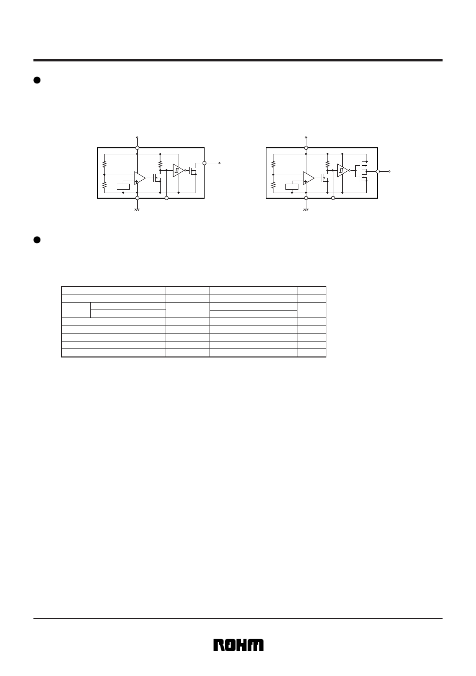
Two output types can be used. One is BD52XXG/FVE (Left) of open drain output type, and the other is
BD53XXG/FVE (Right) of CMOS output type.
• Operating temperature range
The circuit function is guaranteed within the temperature range. However, the operating characteristics are
different from that of Ta=25°C. If they are any questions about the extent of guarantee of circuit functions
in this operating temperature range, please ask for more technical information.
• Output voltage
V
OUT
pin voltage should not exceed the indicated value. For Nch open drain output type, V
DD
applied
voltage and V
OUT
pin H output voltage can be used independently. Both of them should not exceed the
each indicated value.
• Power supply voltage
This voltage is the applied voltage between V
DD
and GND. The applied voltage should not exceed
the indicated value.
• Storage temperature range
This IC can be stored up to this temperature range without deterioration of characteristics. However, an
abrupt thermal shock of extreme temperature fluctuations may cause the deterioration of characteristics.
BD52XXG/FVE : Open drain output
BD53XXG/FVE : CMOS output
Fig.4
Fig.3
Block diagram
Absolute maximum rating (Ta=25°C)
3/15
Voltage detectors
BD52XXG/FVE
BD53XXG/FVE
Vout
Reset
V
DD
V
DD
GND
CT
Vref
Reset
V
DD
Vout
V
DD
GND
CT
Vref
*1 Derating : 5.4mW/°C for operation above Ta=25°C
*2 Derating : 2.1mW/°C for operation above Ta=25°C
*3 When ROHM's standard board(70mmX70mmX1.6mm, glass epoxy board) is mounted.
Power dissipation
(SSOP5(SMP5C2))
Power dissipation
(VSOF5(EMP5))
Operating temperature
Parameter
Symbol
Unit
V
OUT
Pd
Pd
T
opr
V
mW
mW
Storage temperature
T
stg
Limits
– 40 to + 85
– 55 to + 125
540
CT pin voltage
V
CT
V
GND – 0.3 to V
DD
+ 0.3
210
GND – 0.3 to + 10
GND – 0.3 to V
DD
+ 0.3
°C
°C
V
DD
– GND
– 0.3 to + 10
V
*1
*3
*2
*3
Output
voltage
Nch Open drain output
CMOS output
Power supply voltage
Rev.A