Rainbow Electronics DS2761 User Manual
Page 11
DS2761
11 of 24
MEMORY
The DS2761 has a 256-byte linear address space with registers for instrumentation, status, and control in
the lower 32 bytes, with lockable EEPROM and SRAM memory occupying portions of the remaining
address space. All EEPROM and SRAM memory is general purpose except addresses 30h, 31h, and 33h,
which should be written with the default values for the protection register, status register, and current
offset register, respectively. When the MSB of any two-byte register is read, both the MSB and LSB are
latched and held for the duration of the read data command to prevent updates during the read and ensure
synchronization between the two register bytes. For consistent results, always read the MSB and the LSB
of a two-byte register during the same read data command sequence.
EEPROM memory is shadowed by RAM to eliminate programming delays between writes and to allow
the data to be verified by the host system before being copied to EEPROM. All reads and writes to/from
EEPROM memory actually access the shadow RAM. In unlocked EEPROM blocks, the write data
command updates shadow RAM. In locked EEPROM blocks, the write data command is ignored. The
copy data command copies the contents of shadow RAM to EEPROM in an unlocked block of EEPROM
but has no effect on locked blocks. The recall data command copies the contents of a block of EEPROM
to shadow RAM regardless of whether the block is locked or not.
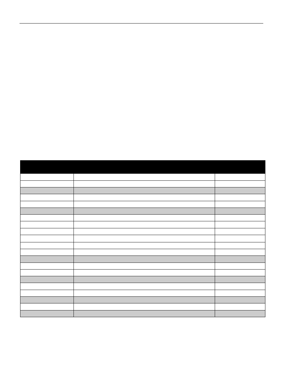
Table 3. MEMORY MAP
ADDRESS (HEX)
DESCRIPTION
READ/WRITE
00
Protection Register
R/W
01
Status Register
R
02–06
Reserved
07
EEPROM Register
R/W
08
Special Feature Register
R/W
09–0B
Reserved
0C
Voltage Register MSB
R
0D
Voltage Register LSB
R
0E
Current Register MSB
R
0F
Current Register LSB
R
10
Accumulated Current Register MSB
R/W
11
Accumulated Current Register LSB
R/W
12–17
Reserved
18
Temperature Register MSB
R
19
Temperature Register LSB
R
1A–1F
Reserved
20–2F
EEPROM, block 0
R/W*
30–3F
EEPROM, block 1
R/W*
40–7F
Reserved
80–8F
SRAM
R/W
90–FF
Reserved
* Each EEPROM block is read/write until locked by the LOCK command, after which it is read-only.