Figure 7. voltage register format, Temperature measurement, Figure 8. temperature register format – Rainbow Electronics DS2761 User Manual
Page 10: Programmable i/o, Power switch input
DS2761
10 of 24
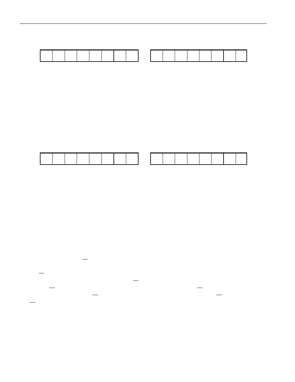
Figure 7. VOLTAGE REGISTER FORMAT
MSB—Address 0C
LSB—Address 0D
S
2
9
2
8
2
7
2
6
2
5
2
4
2
3
2
2
2
1
2
0
X
X
X
X
X
MSb
LSb
MSb
LSb
Units: 4.88mV
TEMPERATURE MEASUREMENT
The DS2761 uses an integrated temperature sensor to continually measure battery temperature.
Temperature measurements are placed in the temperature register every 220ms in two’s-complement
format with a resolution of 0.125°C over a range of
±127°C. The temperature register format is shown in
Figure 8.
Figure 8. TEMPERATURE REGISTER FORMAT
MSB—Address 18
LSB—Address 19
S
2
9
2
8
2
7
2
6
2
5
2
4
2
3
2
2
2
1
2
0
X
X
X
X
X
MSb
LSb
MSb
LSb
Units: 0.125
°C
PROGRAMMABLE I/O
To use the PIO pin as an output, write the desired output value to the PIO bit in the special feature
register. Writing a 0 to the PIO bit enables the PIO output driver, pulling the PIO pin to V
SS
. Writing a 1
to the PIO bit disables the output driver, allowing the PIO pin to be pulled high or used as an input. To
sense the value on the PIO pin, read the PIO bit. The DS2761 turns off the PIO output driver and sets the
PIO bit high when in sleep mode or when DQ is low for more than 2s, regardless of the state of the
PMOD bit.
POWER SWITCH INPUT
The DS2761 provides a power control function that uses the discharge protection FET to gate battery
power to the system. The
PS
pin, internally pulled to V
DD
through a 1
mA current source, is continuously
monitored for a low-impedance connection to V
SS
. If the DS2761 is in sleep mode, the detection of a low
on the
PS
pin causes the device to transition into active mode, turning on the discharge FET. If the
DS2761 is already in active mode, activity on
PS
has no effect other than the latching of its logic low
level in the
PS
bit in the special feature register. The reading of a 0 in the
PS
bit should be immediately
followed by writing a 1 to the
PS
bit to ensure that a subsequent low forced on the
PS
pin is latched into
the
PS
bit.