Ds8024 smart card interface, Clock circuitry, I/o transceivers – Rainbow Electronics DS8024 User Manual
Page 8: Inactive mode, Activation sequence, Table 1. clock frequency selection, Table 2. card presence indication
DS8024
Smart Card Interface
8
_______________________________________________________________________________________
The DS8024 card interface remains inactive no matter
the levels on the command lines until duration t
W
after
V
DD
has reached a level higher than V
TH2
+ V
HYS2
.
When V
DD
falls below V
TH2
, the DS8024 executes a
card deactivation sequence if its card interface is
active.
Clock Circuitry
The clock signal from the DS8024 to the smart card
(CLK) is generated from the clock input on XTAL1 or
from a crystal operating at up to 20MHz connected
between pins XTAL1 and XTAL2. The inputs CLKDIV1
and CLKDIV2 determine the frequency of the CLK sig-
nal, which can be f
XTAL
, f
XTAL/2
, f
XTAL/4
, or f
XTAL/8
.
Table 1 shows the relationship between CLKDIV1 and
CLKDIV2 and the frequency of CLK.
Do not change the state of pins CLKDIV1 and CLKDIV2
simultaneously; a delay of 10ns minimum between
changes is required. The minimum duration of any state
of CLK is 8 periods of XTAL1.
The hardware in the DS8024 guarantees that the fre-
quency change is synchronous. During a transition of
the clock divider, no pulse is shorter than 45% of the
smallest period, and the clock pulses before and after
the instant of change have the correct width.
To achieve a 45% to 55% duty factor on pin CLK when
no crystal is present, the input signal on XTAL1 should
have a 48% to 52% duty factor. Transition time on
XTAL1 should be less than 5% of the period.
With a crystal, the duty factor on pin CLK may be 45%
to 55% depending on the circuit layout and on the crys-
tal characteristics and frequency.
The DS8024 crystal oscillator runs when the device is
powered up. If the crystal oscillator is used or the clock
pulse on pin XTAL1 is permanent, the clock pulse is
applied to the card at time t
4
(see Figures 7 and 8). If
the signal applied to XTAL1 is controlled by the host
microcontroller, the clock pulse is applied to the card
when it is sent by the system microcontroller (after
completion of the activation sequence).
I/O Transceivers
The three data lines I/O, AUX1, and AUX2 are identical.
This section describes the characteristics of I/O and
I/OIN but also applies to AUX1, AUX1IN, AUX2, and
AUX2IN.
I/O and I/OIN are pulled high with an 11k
Ω resistor (I/O
to V
CC
and I/OIN to V
DD
) in the inactive state. The first
side of the transceiver to receive a falling edge
becomes the master. When the master is decided, the
opposite side switches to slave mode, ignoring subse-
quent edges until the master releases. After a time delay
t
D(EDGE)
, an n transistor on the slave side is turned on,
thus transmitting the logic 0 present on the master side.
When the master side asserts a logic 1, a p transistor
on the slave side is activated during the time delay t
PU
and then both sides return to their inactive (pulled up)
states. This active pullup provides fast low-to-high tran-
sitions. After the duration of t
PU
, the output voltage
depends only on the internal pullup resistor and the
load current. Current to and from the card I/O lines is
limited internally to 15mA. The maximum frequency on
these lines is 1MHz.
Inactive Mode
The DS8024 powers up with the card interface in the
inactive mode. Minimal circuitry is active while waiting
for the host to initiate a smart card session.
• All card contacts are inactive (approximately 200
Ω
to GND).
• Pins I/OIN, AUX1IN, and AUX2IN are in the high-
impedance state (11k
Ω pullup resistor to V
DD
).
• Voltage generators are stopped.
• XTAL oscillator is running (if included in the device).
• Voltage supervisor is active.
• The internal oscillator is running at its low frequency.
Activation Sequence
After power-on and the reset delay, the host microcon-
troller can monitor card presence with signals OFF and
CMDVCC, as shown in Table 2.
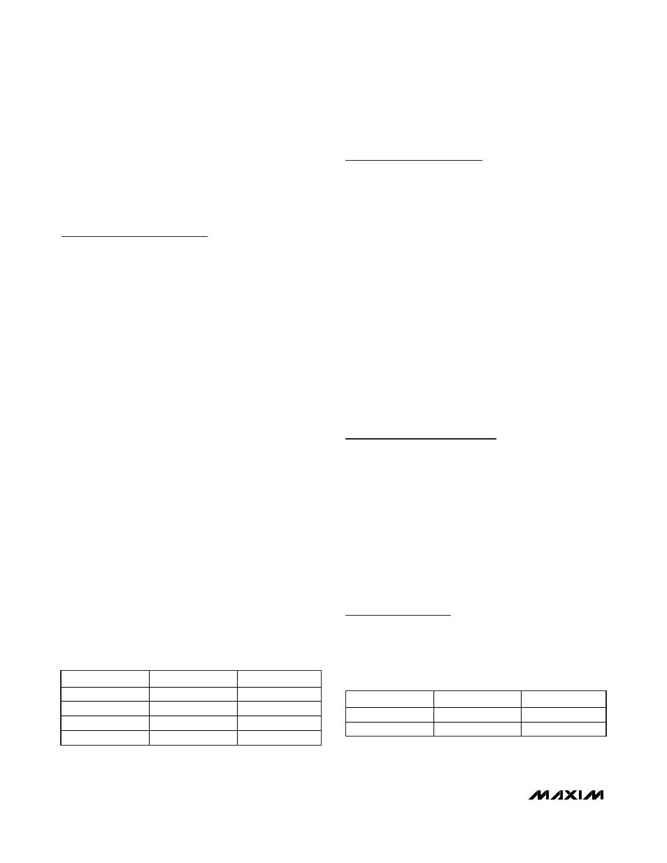
Table 1. Clock Frequency Selection
CLKDIV1
CLKDIV2
f
CLK
0 0
f
XTAL
/8
0 1
f
XTAL
/4
1 1
f
XTAL
/2
1 0
f
XTAL
Table 2. Card Presence Indication
OFF
CMDVCC
STATUS
High High
Card
present.
Low High
Card
not present.