Ds8024 smart card interface – Rainbow Electronics DS8024 User Manual
Page 2
DS8024
Smart Card Interface
2
_______________________________________________________________________________________
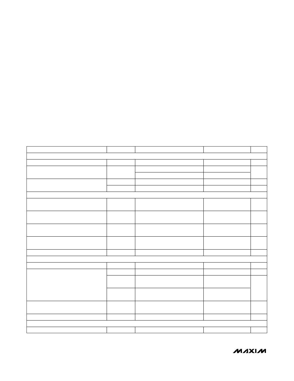
ABSOLUTE MAXIMUM RATINGS
RECOMMENDED DC OPERATING CONDITIONS
(V
DD
= +3.3V, V
DDA
= +5.0V, T
A
= +25°C, unless otherwise noted.) (Note 1)
Stresses beyond those listed under “Absolute Maximum Ratings” may cause permanent damage to the device. These are stress ratings only, and functional
operation of the device at these or any other conditions beyond those indicated in the operational sections of the specifications is not implied. Exposure to
absolute maximum rating conditions for extended periods may affect device reliability.
Voltage Range on V
DD
Relative to GND ...............-0.5V to +6.5V
Voltage Range on V
DDA
Relative to PGND ...........-0.5V to +6.5V
Voltage Range on CP1, CP2, and V
UP
Relative to PGND...............................................-0.5V to +7.5V
Voltage Range on All Other Pins
Relative to GND......................................-0.5V to (V
DD
+ 0.5V)
Maximum Junction Temperature .....................................+125°C
Maximum Power Dissipation (T
A
= -25°C to +85°C) .......700mW
Storage Temperature Range .............................-55°C to +150°C
Soldering Temperature.........Refer to the IPC/JEDEC J-STD-020
Specification.
PARAMETER
SYMBOL
CONDITIONS
MIN
TYP
MAX
UNITS
POWER SUPPLY
Digital Supply Voltage
V
DD
2.7 6.0 V
V
CC
= 5V,
|I
CC
| < 80mA
4.0
6.0
Card Voltage-Generator Supply Voltage
V
DDA
V
CC
= 5V,
|I
CC
| < 30mA
3.0
6.0
V
V
TH2
Threshold voltage (falling)
2.30
2.45
2.60
V
Reset Voltage Thresholds
V
HYS2
Hysteresis
50 100 150 mV
CURRENT CONSUMPTION
Active V
DD
Current 5V Cards
(Including 80mA Draw from 5V Card)
I
DD_50V
I
CC
= 80mA, f
XTAL
= 20MHz,
f
CLK
= 10MHz, V
DDA
= 5.0V
215
mA
Active V
DD
Current 5V Cards
(Current Consumed by DS8024 Only)
I
DD_IC
I
CC
= 80mA, f
XTAL
= 20MHz,
f
CLK
= 10MHz, V
DDA
= 5.0V (Note 2)
135
mA
Active V
DD
Current 3V Cards
(Including 65mA Draw from 3V Card)
I
DD_30V
I
CC
= 65mA, f
XTAL
= 20MHz,
f
CLK
= 10MHz, V
DDA
= 5.0V
100
mA
Active V
DD
Current 3V Cards
(Current Consumed by DS8024 Only)
I
DD_IC
I
CC
= 65mA, f
XTAL
= 20MHz,
f
CLK
= 10MHz, V
DDA
= 5.0V (Note 2)
35
mA
Inactive-Mode Current
I
DD
Card
inactive
500
μA
CLOCK SOURCE
Crystal Frequency
f
XTAL
External
crystal
0 20 MHz
f
XTAL1
0
20
MHz
V
IL_XTAL1
Low-level input on XTAL1 (Note 3)
-0.3
0.3 x
V
DD
XTAL1 Operating Conditions
V
IH_XTAL1
High-level input on XTAL1 (Note 3)
0.7 x
V
DD
V
DD
+
0.3
V
External Capacitance for Crystal
C
XTAL1
,
C
XTAL2
(Note 3)
15
pF
Internal Oscillator
f
INT
2.7 MHz
SHUTDOWN TEMPERATURE
Shutdown Temperature
T
SD
(Note
3)
+150 °C