Rainbow Electronics DS4520 User Manual
Page 7
DS4520
9-Bit I
2
C Nonvolatile
I/O Expander Plus Memory
_____________________________________________________________________
7
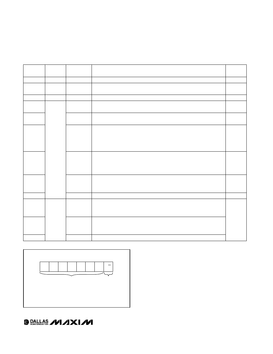
*THE SLAVE ADDRESS IS DETERMINED BY
ADDRESS PINS A0, A1, AND A2.
1
MSB
SLAVE
ADDRESS*
READ/WRITE
BIT
LSB
0
1
0
A2
A1
A0
R/W
Figure 1. DS4520 Slave Address Byte
Table 1. DS4520 Memory Map
ADDRESS
TYPE
NAME
FUNCTION
FACTORY
DEFAULT
00h to 3Fh
EEPROM
User Memory 64 bytes of general-purpose user EEPROM.
00h
40 to E7h
—
Reserved
Undefined address space for future expansion. Reads and writes to this
space have no effect on the device.
—
E8 to EFh
EEPROM
Reserved
—
—
F0h
Pullup
Enable 0
Pullup enable for I/O_0 to I/O_7. I/O_0 is the LSB and I/O_7 is the MSB. Set
the corresponding bit to enable the pullup; clear the bit to disable the pullup.
00h
F1h
Pullup
Enable 1
Pullup enable for I/O_8. I/O_8 is the LSB. Only the LSB is used. Set the LSB
bit to enable the pullup on I/O_8; clear the LSB to disable the pullup.
00h
F2h
I/O Control 0
I/O control for I/O_0 to I/O_7. I/O_0 is the LSB and I/O_7 is the MSB. Clearing
the corresponding bit of the register pulls the selected I/O pin low; setting the
bit places the pulldown transistor into a high-impedance state. When the
pulldown is high impedance, the output floats if no pullup/down is connected
to the pin.
FFh
F3h
I/O Control 1
I/O control for I/O_8. I/O_8 is the LSB. Only the LSB is used. Clearing the LSB
of the register pulls the I/O_8 pin low; setting the LSB places the pulldown
transistor into a high-impedance state. When the pulldown is high impedance,
the output floats if no pullup/down is connected to the pin.
01h
F4h
Configuration
Configuration register. The LSB is the SEE bit. When set, this bit disables
writes to the EEPROM; writing only affects the shadow SRAM. When set to 0,
both the EEPROM and the shadow SRAM is written.
00h
F5h to F7h
SRAM
Shadowed
EEPROM
[EEPROM
writes are
disabled if
the SEE
bit = 1]
User Memory 3 bytes of general-purpose user EEPROM.
00h
F8h
I/O Status 0
I/O status for I/O_0 to I/O_7. I/O_0 is the LSB and I/O_7 is the MSB. Writing to
this register has no effect. Read this register to determine the state of the
I/O_0 to I/O_7 pins.
F9h
I/O Status 1
I/O status for I/O_8. I/O_8 is the LSB. Only the LSB is used; the other bits
could be any value when read. Writing to this register has no effect. Read this
register to determine the state of the I/O_8 pin.
FAh to FFh
SRAM
SRAM User
6 bytes of general-purpose SRAM.
—