Applications information, Chip topology, Package information – Rainbow Electronics DS4520 User Manual
Page 10: Power-supply decoupling, And gnd pins of the ic to minimize lead inductance
DS4520
9-Bit I
2
C Nonvolatile
I/O Expander Plus Memory
Maxim cannot assume responsibility for use of any circuitry other than circuitry entirely embodied in a Maxim product. No circuit patent licenses are
implied. Maxim reserves the right to change the circuitry and specifications without notice at any time.
10
____________________Maxim Integrated Products, 120 San Gabriel Drive, Sunnyvale, CA 94086 408-737-7600
© 2004 Maxim Integrated Products
Printed USA
is a registered trademark of Maxim Integrated Products.
is a registered trademark of Dallas Semiconductor Corporation.
SLAVE
ADDRESS*
START
START
1
0
1
0
A2
A1
A0 R/W
SLAVE
ACK
SLAVE
ACK
SLAVE
ACK
MSB
LSB
MSB
LSB
MSB
LSB
b7
b6
b5
b4
b3
b2
b1
b0
READ/
WRITE
REGISTER ADDRESS
b7
b6
b5
b4
b3
b2
b1
b0
DATA
STOP
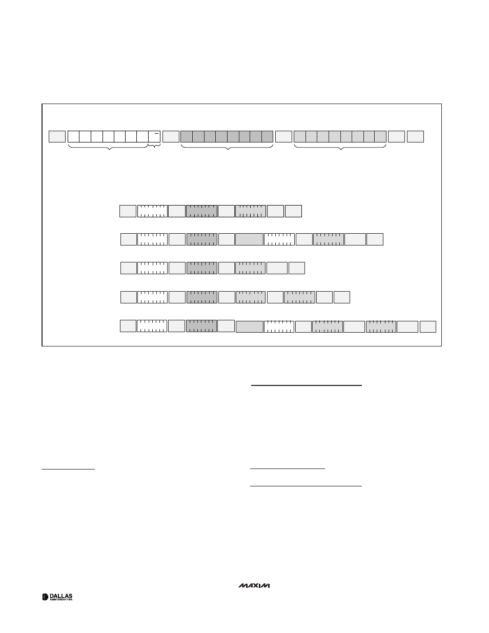
SINGLE BYTE WRITE
-WRITE I/O CONTROL 0
REGISTER TO 00h
SINGLE BYTE WRITE
-WRITE PULLUP ENABLE 0
REGISTER TO FFh
SINGLE BYTE READ
-READ I/O STATUS 0 RESISTER
TWO BYTE WRITE
-WRITE I/O CONTROL 0 AND
I/O CONTROL 1 REGISTERS TO 00h
START
STOP
1 0 1 0 0 0 0 0
1 1 1 1 0 0 1 0
A0h
F2h
START
REPEATED
START
A1h
MASTER
NACK
STOP
1 0 1 0 0 0 0 0
1 1 1 1 1 0 0 0
F8h
1 0 1 0 0 0 0 1
1 0 1 0 0 0 0 0
1 1 1 1 0 0 1 0
A0h
F2h
STOP
I/O STATUS
START 1 0 1 0 0 0 0 0
1 1 1 1 0 0 0 0
A0h
F0h
STOP
DATA
FFh
00h
00h
EXAMPLE I
2
C TRANSACTIONS (WHEN A0, A1, AND A2 ARE CONNECTED TO GND)
TYPICAL I
2
C WRITE TRANSACTION
*THE SLAVE ADDRESS IS DETERMINED BY ADDRESS PINS A0, A1, AND A2.
0 0 0 0 0 0 0 0
1 1 1 1 1 1 1 1
A0h
0 0 0 0 0 0 0 0
TWO BYTE READ
-READ I/O STATUS 0 AND I/O
STATUS 1 RGISTERS
A)
C)
B)
D)
D)
START
STOP
1 0 1 0 0 0 0 0
1 1 1 1 1 0 0 0
A0h
F8h
A1h
1 0 1 0 0 0 0 1
I/O STATUS 0
DATA
I/O STATUS 1
DATA
SLAVE
ACK
SLAVE
ACK
SLAVE
ACK
SLAVE
ACK
SLAVE
ACK
SLAVE
ACK
SLAVE
ACK
SLAVE
ACK
SLAVE
ACK
SLAVE
ACK
SLAVE
ACK
SLAVE
ACK
SLAVE
ACK
SLAVE
ACK
SLAVE
ACK
SLAVE
ACK
MASTER
ACK
MASTER
NACK
REPEATED
START
0 0 0 0 0 0 0 0
Figure 3. I
2
C Communication Examples
See Figure 3 for a read example using the repeated
start condition to specify the starting memory location.
Reading Multiple Bytes from a Slave: The read oper-
ation can be used to read multiple bytes with a single
transfer. When reading bytes from the slave, the master
simply ACKs the data byte if it desires to read another
byte before terminating the transaction. After the mas-
ter reads the last byte it must NACK to indicate the end
of the transfer and generates a stop condition.
Applications Information
Power-Supply Decoupling
To achieve best results, it is highly recommended that a
decoupling capacitor is used on the IC power-supply
pins. Typical values of decoupling capacitors are 0.01µF
and 0.1µF. Use a high-quality, ceramic, surface-mount
capacitor, and mount it as close as possible to the V
CC
and GND pins of the IC to minimize lead inductance.
Chip Topology
TRANSISTOR COUNT: 14,398
SUBSTRATE CONNECTED TO GROUND
Package Information
For the latest package outline information, go to
www.maxim-ic.com/DallasPackInfo
.