Ac electrical characteristics (see figure 2) – Rainbow Electronics DS4520 User Manual
Page 3
DS4520
9-Bit I
2
C Nonvolatile
I/O Expander Plus Memory
_____________________________________________________________________
3
Note 1: All voltages referenced to ground.
Note 2: I
STBY
is specified with SDA = SCL = V
CC
, outputs floating, and inputs connected to V
CC
or GND.
Note 3: The DS4520 does not obstruct the SDA and SCL lines if V
CC
is switched off as long as the voltages applied to these inputs
do not violate their minimum and maximum input voltage levels.
Note 4: Guaranteed by design.
Note 5: Timing shown is for fast-mode (400kHz) operation. This device is also backward compatible with I
2
C standard-mode timing.
Note 6: C
B
—total capacitance of one bus line in picofarads.
Note 7: EEPROM write time applies to all the EEPROM memory and SRAM shadowed EEPROM memory when SEE = 0. The EEPROM
write time begins after a stop condition occurs.
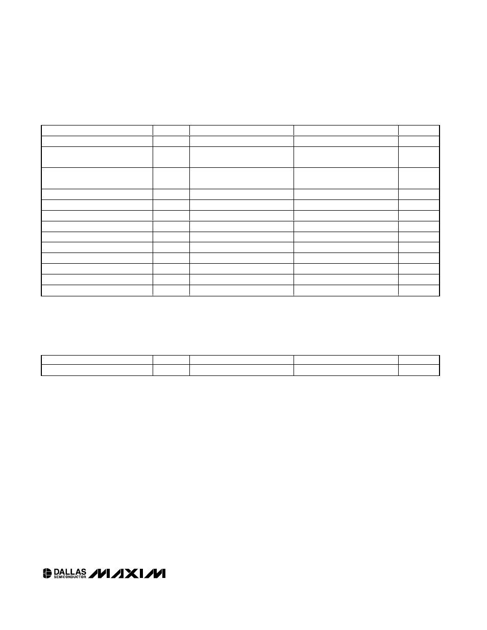
AC ELECTRICAL CHARACTERISTICS (See Figure 2)
(V
CC
= +2.7V to +5.5V; T
A
= -40°C to +85°C, unless otherwise noted. Timing referenced to V
IL(MAX)
and V
IH(MIN)
.)
PARAMETER
SYMBOL
CONDITIONS
MIN
TYP
MAX
UNITS
SCL Clock Frequency
f
SCL
(Note 5)
0
400
kHz
Bus Free Time Between Stop and
Start Conditions
t
BUF
1.3
µs
Hold Time (Repeated) Start
Condition
t
HD:STA
0.6
µs
Low Period of SCL
t
LOW
1.3
µs
High Period of SCL
t
HIGH
0.6
µs
Data Hold Time
t
HD:DAT
0
0.9
µs
Data Setup Time
t
SU:DAT
100
ns
Start Setup time
t
SU:STA
0.6
µs
SDA and SCL Rise Time
t
R
(Note 6)
20 + 0.1C
B
300
ns
SDA and SCL Fall Time
t
F
(Note 6)
20 + 0.1C
B
300
ns
Stop Setup Time
t
SU:STO
0.6
µs
SDA and SCL Capacitive Loading
C
B
(Note 6)
400
pF
EEPROM Write Time
t
WR
(Note 7)
10
20
ms
NONVOLATILE MEMORY CHARACTERISTICS
(V
CC
= +2.7V to +5.5V, unless otherwise noted.)
PARAMETER
SYMBOL
CONDITIONS
MIN
TYP
MAX
UNITS
EEPROM Writes
+70°C (Note 4)
50,000