Pin description, Block diagram – Rainbow Electronics DS4520 User Manual
Page 5
DS4520
9-Bit I
2
C Nonvolatile
I/O Expander Plus Memory
_____________________________________________________________________
5
Pin Description
PIN
NAME
FUNCTION
1
I/O_0
Input/Output 0. Bidirectional I/O pin.
2
I/O_1
Input/Output 1. Bidirectional I/O pin.
3
I/O_2
Input/Output 2. Bidirectional I/O pin.
4
I/O_3
Input/Output 3. Bidirectional I/O pin.
5
I/O_4
Input/Output 4. Bidirectional I/O pin.
6
A0
I
2
C Address Input. Inputs A0, A1, and A2 determine the I
2
C slave address of the device.
7
A1
I
2
C Address Input. Inputs A0, A1, and A2 determine the I
2
C slave address of the device.
8
V
CC
Power-Supply Voltage
9
SDA
I
2
C Serial Data Open-Drain Input/Output
10
SCL
I
2
C Serial Clock Input
11
A2
I
2
C Address Input. Inputs A0, A1, and A2 determine the I
2
C slave address of the device.
12
I/O_5
Input/Output 5. Bidirectional I/O pin.
13
I/O_6
Input/Output 6. Bidirectional I/O pin.
14
I/O_7
Input/Output 7. Bidirectional I/O pin.
15
I/O_8
Input/Output 8. Bidirectional I/O pin.
16
GND
Ground
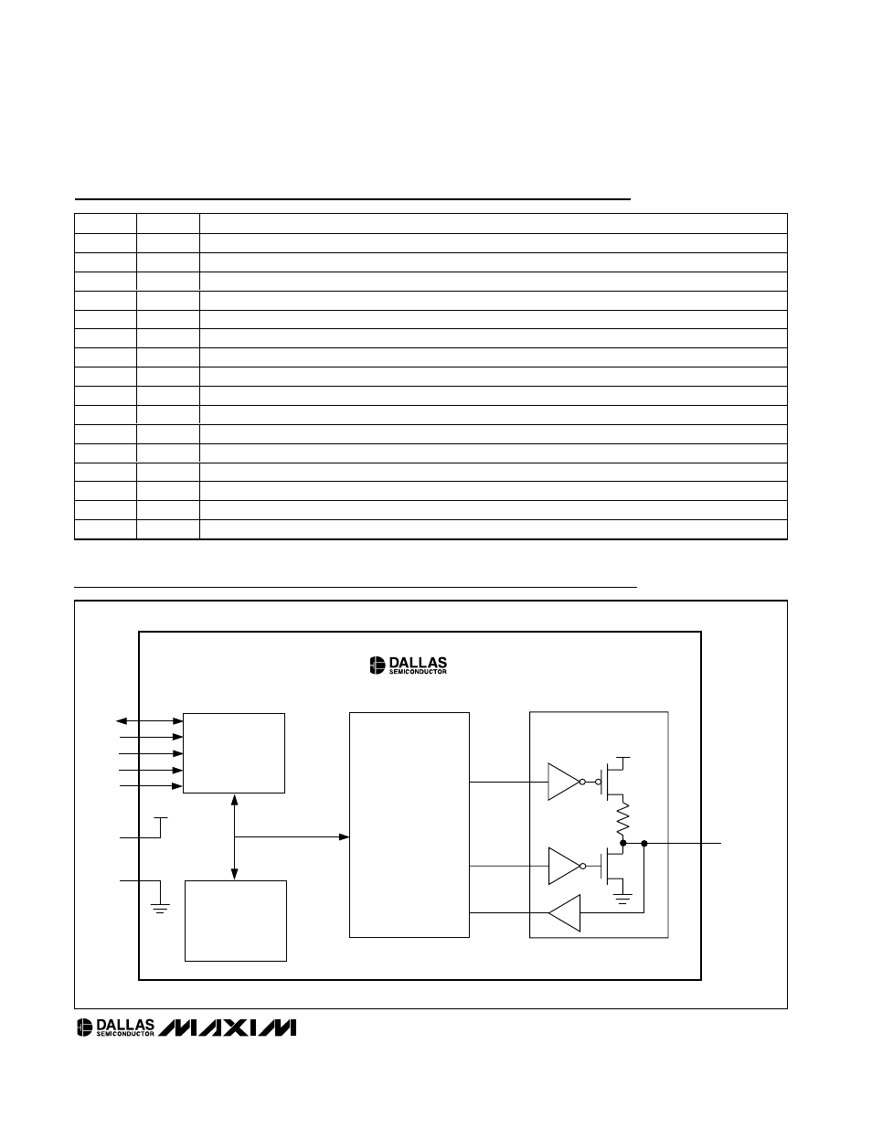
DS4520
I/O CONTROL
REGISTERS
I/O CELL (x9)
I/O_n
[n = 0 TO 8]
R
PU
PULLUP ENABLE (F0h-F1h)
I/O CONTROL (F2h-F3h)
I/O STATUS (F8h-F9h)
I
2
C
INTERFACE
SDA
SCL
A0
A1
A2
GND
EEPROM
64 BYTES
USER MEMORY
[00h TO 3Fh]
V
CC
V
CC
V
CC
Block Diagram