Atr0601 [preliminary, Pin configuration – Rainbow Electronics ATR0601 User Manual
Page 2
2
4866A–GPS–08/05
ATR0601 [Preliminary]
2.
Pin Configuration
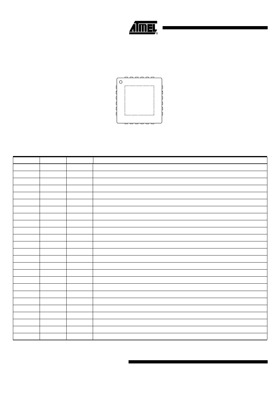
Figure 2-1.
Pinning QFN24
1
2
3
4
5
6
18
17
16
15
14
13
7 8 9 10 11 12
24 23 22 21 20 19
Paddle
GND
VDIG
AGCO
NXTO
NX
X
XTO
PURF
PUXTO
NBPI
BPI
NBP
BP
VC
C
MO
TEST
NRF
RF
NC
SC
SH
SL
SD
I
EG
C
VC
C
Table 2-1.
Pin Description
Pin
Symbol
Type
(1)
Function
Paddle
GND
S
Common ground
1
VDIG
S
Digital supply
2
AGCO
A_I/O
AGC: gain control voltage output/corner frequency determination
3
NXTO
A_I
XTO interface (optional: TCXO input)
4
NX
A_O
XTO interface
5
X
A_O
XTO interface
6
XTO
A_I
XTO interface (optional: TCXO input)
7
VCC
S
Analog supply
8
MO
A_O
Testbuffer output (f
IF
)
9
TEST
A_I
Enable testbuffer
10
NRF
A_I
RF input complementary
11
RF
A_I
RF input
12
NC
–
Not connected
13
BP
A_O
IF-Filter interface (mixer output, open collector)
14
NBP
A_O
IF-Filter interface (mixer output complementary, open collector)
15
BPI
A_I
IF-Filter interface (IF-input)
16
NBPI
A_I
IF-Filter interface (IF-input complementary)
17
PUXTO
D_I
Power-up XTO
18
PURF
D_I
Power-up RF
19
VCC
S
Analog supply
20
EGC
D_I
Enable external gain control (high = external; low = internal)
21
SDI
D_I
Input for external gain control signal (
Σ∆
modulation)
22
SL
D_O
Data output: “low”
23
SH
D_O
Data output: “high”
24
SC
D_O
Sample clock
Note:
1. Type: A_I Analog input, A_O Analog output, D_I Digital input, D_O Digital output, S Supply