Rainbow Electronics ATA6286 User Manual
Page 16
16
4958AS–AUTO–09/06
ATA6285/ATA6286 [Preliminary]
4.5.5.1
Clock Pulse Take-over by Microcontroller
The clock of the crystal oscillator can be used for clocking the microcontroller. Atmel’s ATARx9x
microcontroller family provides the special feature of starting with an integrated RC oscillator to
switch on the ATA6285/ATA6286 external clocking and to wait automatically until the CLK out-
put of the ATA6285/ATA6286 is activated. After a time period of 250 µs the message can be
sent with crystal accuracy.
4.5.6
Output Matching and Power Setting
The output power is set by the load impedance of the antenna. The maximum output power is
achieved with a load impedance of Z
Load, opt
= 380
Ω
+ j340
Ω
(ATA6286) at 315 MHz and
Z
Load, opt
= 280
Ω
+ j310
Ω
(ATA6285) at 433.92 MHz. A low resistive path to V
S
is required to
deliver the DC current.
The power amplifier delivers a current pulse and the maximum output power is delivered to a
resistive load if the 0.66 pF output capacitance of the power amplifier is compensated by the
load impedance.
At the ANT1 pin, the RF output amplitude is about V
S
– 0.5V.
The load impedance is defined as the impedance seen from the ATA6285’s ANT1, ANT2 into
the matching network. Do not mix up this large-signal load impedance with a small-signal input
impedance delivered as an input characteristic of RF amplifiers.
The latter is measured from the application into the IC instead of from the IC into the application
for a power amplifier.
The 0.66 pF output capacitance absorbed into the load impedance a real impedance of 684
Ω
(ATA6285) at 315 MHz and 623
Ω
(ATA6286) at 433.92 MHz should be measured with a network
analyses at pin 5 (ANT1) with the ATA6285/ATA6286 soldered, an optimized antenna con-
nected and the power amplifier switched off.
Less output power is achieved by lowering the real parallel part where the parallel imaginary part
should be kept constant. Lowering the real part of the load impedance also reduces the supply
voltage dependency of the output power.
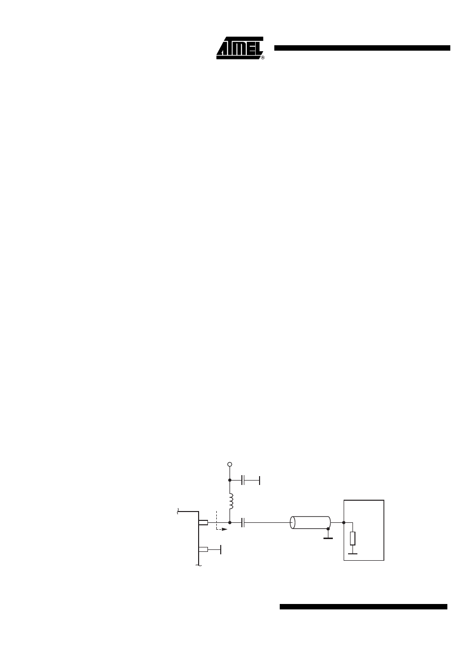
Output power measurement can be done with the circuit as shown in Output Power Measure-
ment. Please note that the component values must be changed to compensate the individual
board parasitics until the ATA6285/ATA6286 has the right load impedance. Also, the damping of
the cable used to measure the output power must be calibrated.
Figure 4-7.
Output Power Measurement ATA6285/ATA6286
L
1
= 68 nH/ 39 nH
C
2
= 2.2 pF/ 1.8 pF
C
1
= 1 nF
V
S
R
in
ANT2
ANT1
Z
Lopt
Power
meter
50
Ω
Z = 50
Ω